
Datasheet


Dataline
stable;
datavalid
SDAT
SCLK
Change
ofdata
allowed
SDAT
STARTcondition
SCLK
STOP condition
TPS65720
TPS65721
www.ti.com
SLVS979 –OCTOBER 2009
INT Output
Actively low, open drain interrupt output. Connect external pull-up resistor. Interrupts are flagged in the registers
IR0, IR1 and IR2 if the interrupt is not masked by registers IRMASK0, IRMASK1 and IRMASK2. Per default, all
interrupts are masked. Interrupts which are unmasked will set the Bit in either on the rising edge or on both
edges. Details can be found in the register description for IR0, IR1 and IR2. Any Bit in IR0, IR1 and IR2, set to
“1” will drive the reset pin INT actively LOW.
The reset pin will go high impedance after the Bit, generating the reset is read.
Serial Interface
The serial interface is compatible with the standard and fast mode I2C specifications, allowing transfers at up to
400kHz. The interface adds flexibility to the power supply solution, enabling most functions to be programmed to
new values depending on the instantaneous application requirements and charger status to be monitored.
Register contents remain intact as long as VCC remains above the UVLO threshold. The TPS65720 has a 7bit
address: ‘100 1000’, other addresses are available upon contact with the factory. Attempting to read data from
register addresses not listed in this section will result in 00h being read out.
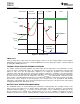
For normal data transfer, DATA is allowed to change only when CLK is low. Changes when CLK is high are
reserved for indicating the start and stop conditions. During data transfer, the data line must remain stable
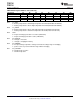
whenever the clock line is high. There is one clock pulse per bit of data. Each data transfer is initiated with a start
condition and terminated with a stop condition. When addressed, the TPS65720 device generates an
acknowledge bit after the reception of each byte. The master device (microprocessor) must generate an extra
clock pulse that is associated with the acknowledge bit. The TPS65720 device must pull down the DATA line
during the acknowledge clock pulse so that the DATA line is a stable low during the high period of the
acknowledge clock pulse. The DATA line is a stable low during the high period of the acknowledge–related clock
pulse. Setup and hold times must be taken into account. During read operations, a master must signal the end of
data to the slave by not generating an acknowledge bit on the last byte that was clocked out of the slave. In this
case, the slave TPS65720 device must leave the data line high to enable the master to generate the stop
condition.
For the QFN version, the voltage the pull-up resistors for the I2C interface at SCLK and SDAT are connected to,
should be monitored by the reset circuitry. This is done by connecting THRESHOLD with a voltage divider to the
voltage the SDAT and SCLK pins are pulled-up to. This is needed to ensure a falling supply voltage will cause a
reset to the I2C interface. Otherwise a START condition may be detected and the first access to the I2C interface
may return NO ACK (no acknowledge).
Figure 28. Bit Transfer on the Serial Interface
Figure 29. START and STOP Conditions
Copyright © 2009, Texas Instruments Incorporated Submit Documentation Feedback 27
Product Folder Link(s): TPS65720 TPS65721