
Datasheet

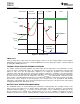


TPS65720
TPS65721
www.ti.com
SLVS979 –OCTOBER 2009
window, charging is resumed and the timers continue counting. When charging is suspended due to a battery
pack temperature fault, the CH_ACTIVE Bit remains 1 and continues to indicate charging. Battery pack
temperature sensing is disabled when termination is disabled (<TERM_EN=0>) and the voltage at TS is greater
than V
DIS(TS)
. The battery pack temperature monitoring is disabled by connecting a 10-kΩ resistor from TS to
GND.
TPS65720 contains a feature to shift the termination temperature to higher levels by setting Bits <TMP_SHIFT1,
TMP_SHIFT0>.
DCDC1 CONVERTER
The TPS65720 step down converter operates with typically 2.25 MHz fixed frequency pulse width modulation
(PWM) at moderate to heavy load currents. At light load currents the converter can automatically enter Power
Save Mode and operates then in PFM mode.
During PWM operation the converter use a unique fast response voltage mode control scheme with input voltage
feed-forward to achieve good line and load regulation allowing the use of small ceramic input and output
capacitors. At the beginning of each clock cycle initiated by the clock signal, the High Side MOSFET switch is
turned on. The current flows now from the input capacitor via the High Side MOSFET switch through the inductor
to the output capacitor and load. During this phase, the current ramps up until the PWM comparator trips and the
control logic will turn off the switch. The current limit comparator will also turn off the switch in case the current
limit of the High Side MOSFET switch is exceeded. After a dead time preventing shoot through current, the Low
Side MOSFET rectifier is turned on and the inductor current will ramp down. The current flows now from the
inductor to the output capacitor and to the load. It returns back to the inductor through the Low Side MOSFET
rectifier.
The next cycle will be initiated by the clock signal again turning off the Low Side MOSFET rectifier and turning on
the on the High Side MOSFET switch.
The DCDC1 converters output voltage is externally adjustable using a resistor divider at FB_DCDC1.
POWER SAVE MODE
The Power Save Mode is enabled automatically with <F_PWM>=0 which is the default setting. If the load current
decreases, the converter will enter Power Save Mode operation automatically. During Power Save Mode the
converter skips switching and operates with reduced frequency in PFM mode with a minimum quiescent current
to maintain high efficiency. The converter will position the output voltage typically +1% above the nominal output
voltage. This voltage positioning feature minimizes voltage drops caused by a sudden load step. The transition
from PWM mode to PFM mode occurs once the inductor current in the Low Side MOSFET switch becomes zero,
which indicates discontinuous conduction mode. During the Power Save Mode the output voltage is monitored
with a PFM comparator. As the output voltage falls below the PFM comparator threshold of VOUT nominal +1%,
the device starts a PFM current pulse. The High Side MOSFET switch will turn on, and the inductor current
ramps up. After the On-time expires, the switch is turned off and the Low Side MOSFET switch is turned on until
the inductor current becomes zero. The converter effectively delivers a current to the output capacitor and the
load. If the load is below the delivered current, the output voltage will rise. If the output voltage is equal or higher
than the PFM comparator threshold, the device stops switching and enters a sleep mode with typical 15μA
current consumption.
If the output voltage is still below the PFM comparator threshold, a sequence of further PFM current pulses are
generated until the PFM comparator threshold is reached. The converter starts switching again once the output
voltage drops below the PFM comparator threshold. With a fast single threshold comparator, the output voltage
ripple during PFM mode operation can be kept small. The PFM Pulse is time controlled, which allows to modify
the charge transferred to the output capacitor by the value of the inductor. The resulting PFM output voltage
ripple and PFM frequency depend in first order on the size of the output capacitor and the inductor value.
Increasing output capacitor values and inductor values will minimize the output ripple. The PFM frequency
decreases with smaller inductor values and increases with larger values. The PFM mode is left and PWM mode
is entered in case the output current can not longer be supported in PFM mode. The Power Save Mode can be
disabled by setting <F_PWM>=1. The converter will then operate in fixed frequency PWM mode.
Copyright © 2009, Texas Instruments Incorporated Submit Documentation Feedback 23
Product Folder Link(s): TPS65720 TPS65721