
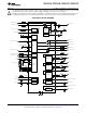
Datasheet


LS2_OUT – 43
LS1_IN – 39
nRESET – 44
nINT – 45
LDO_PGOOD – 46
BYPASS – 47
INT_LDO – 48
VLDO2 – 1
VINLDO – 2
VLDO1 – 3
BAT – 4
BAT – 5
BAT_SENSE – 6
SYS – 7
19 – VDCDC1
18 – VIO
17 – NC
16 – MUX_OUT
15 – NC
14 – MUX_IN
13 – nWAKEUP
48-PIN 6mm x6mm x 1mm QFN
RSL PACKAGE
(TOP VIEW)
SYS – 8
PWR_EN – 9
AC – 10
TS – 11
USB – 12
24 – VDCDC2
23 – L2
22 – VIN_DCDC2
21 – VIN_DCDC1
20 – L1
31 – L3
30 – PGND
29 – VDCDC3
28 – SCL
27 – SDA
26 – PGOOD
25 – PB_IN
36 – ISET2
35 – ISET1
34 – ISINK1
33 – ISINK2
32 – VIN_DCDC3
L4 – 37
FB_WLED – 38
LS1_OUT – 40
AGND – 41
LS2_IN – 42
x = CHIP DESIGNATOR (A, B, or C)
TI = TI LETTERS
YM = YEAR / MONTH DATE CODE
LLLL = LOT TRACE CODE
S = ASSEMBLY SITE CODE
O = Pin 1 (MARKED)
TPS
65217x
TI YMS
LLLL G4
TPS65217A, TPS65217B, TPS65217C, TPS65217D
www.ti.com
SLVSB64F –NOVEMBER 2011–REVISED APRIL 2013
DEVICE INFORMATION
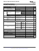
TERMINAL FUNCTIONS
TERMINAL
I/O DESCRIPTION
NAME NO.
VLDO2 1 O Output voltage of LDO2
VINLDO 2 I Input voltage for LDO1 and LDO2
VLDO1 3 O Output voltage of LDO1
BAT 4, 5 I/O Battery charger output. Connect to battery.
BAT_SENSE 6 I Battery voltage sense input, connect to BAT directly at the battery terminal.
System voltage pin and output of the power path. All voltage regulators are typically
SYS 7, 8 O
powered from this output.
Enable input for DCDC1, 2, 3 converters and LDO1, 2, 3, 4. Pull this pin high to start the
PWR_EN 9 I
power-up sequence.
AC 10 I AC adapter input to power path. Connect to an external DC supply.
Temperature sense input. Connect to NTC thermistor to sense battery temperature.
TS 11 I
Works with 10k and 100k thermistors. See charger section for details.
USB 12 I USB voltage input to power path. Connect to external voltage from a USB port.
nWAKEUP 13 O Signal to host to indicate a power on event (active low, open-drain output)
MUX_IN 14 O Input to analog multiplexer
NC 15 Not used
MUX_OUT 16 O Output pin of analog multiplexer
NC 17 Not used
VIO 18 I Output-high supply for output buffers
VDCDC1 19 I DCDC1 output/ feedback voltage sense input
Copyright © 2011–2013, Texas Instruments Incorporated Submit Documentation Feedback 5
Product Folder Links: TPS65217A TPS65217B TPS65217C TPS65217D