
Datasheet


www.ti.com
0
0.02
0.04
0.06
0.08
0.10
0.12
0.14
9
10 11 12 13 14 15
Vo1 − Output Voltage − V
− Output Current − AI
O
Vo3 = 18 V (Doubler Mode)
T
A
= 25°C
T
A
= 85°C
T
A
= −40°C
0
0.02
0.04
0.06
0.08
0.10
0.12
9
10 11 12 13 14 15
Vo1 − Output Voltage − V
− Output Current − AI
O
Vo3 = 28 V (Tripler Mode)
T
A
= 25°C
T
A
= 85°C
T
A
= −40°C
DETAILED DESCRIPTION
Main Boost Converter
VCOM Buffer
Enable and Power On Sequencing (EN, ENR)
TPS65100 , TPS65101
TPS65105
SLVS496C – SEPTEMBER 2003 – REVISED APRIL 2006
V
O
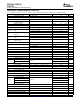
3 MAXIMUM LOAD CURRENT V
O
3 MAXIMUM LOAD CURRENT
Figure 13. Figure 14.
The TPS6510x series consists of a main boost converter operating with a fixed switching frequency of 1.6 MHz
to allow for small external components. The boost converter output voltage V
O
1 is also the input voltage,
connected via the pin SUP, for the positive and negative charge pumps and the bias supply for the VCOM
buffer. The linear regulator controller is independent from this system with its own enable pin. This allows the
linear regulator controller to continue to operate while the other supply rails are disabled or in shutdown due to a
fault condition on one of their outputs. See the functional block diagram for more information.
The main boost converter operates with PWM and a fixed switching frequency of 1.6 MHz. The converter uses a
unique fast response, voltage mode controller scheme with input voltage feedforward. This achieves excellent
line and load regulation (0.2% A load regulation typical) and allows the use of small external components. To
add higher flexibility to the selection of external component values the device uses external loop compensation.
Although the boost converter looks like a nonsynchronous boost converter topology operating in discontinuous
mode at light load, the TPS6510x series maintains continuous conduction even at light load currents. This is
accoplished using the Virtual Synchronous Converter Technology for improved load transient response. This
architecture uses an external Schottky diode and an integrated MOSFET in parallel connected between SW and
SUP (see the functional block diagram). The integrated MOSFET Q2 allows the inductor current to become
negative at light load conditions. For this purpose, a small integrated P-channel MOSFET with typically 10 Ω
r
DSon
is sufficient. When the inductor current is positive, the external Schottky diode with the lower forward
voltage conducts the current. This causes the converter to operate with a fixed frequency in continuous
conduction mode over the entire load current range. This avoids the ringing on the switch pin as seen with a
standard nonsynchronous boost converter and allows a simpler compensation for the boost converter.
VCOMIN is the input of the VCOM buffer. If the VCOM buffer is not required for certain applications, it is
possible to shut down the VCOM buffer by statically connecting VCOMIN to ground, reducing the overall
quiescent current. The VCOM buffer features soft start avoiding a large voltage drop at V
O
1 during start-up. The
VCOMIN cannot be pulled dynamically to ground during operation.
The device has two enable pins. These pins should be terminated and not left floating to prevent unpredictable
operation. Pulling the enable pin (EN) high enables the device and starts the power on sequencing with the main
boost converter V
O
1 coming up first then the negative and positive charge pump and the VCOM buffer. If the
VCOMIN pin is held low, the VCOM buffer remains disabled. The linear regulator has an independent enable pin
(ENR). Pulling this pin low disables the regulator, and pulling this pin high enables this regulator.
If the enable pin EN is pulled high, the device starts its power on sequencing. The main boost converter starts
up first with its soft start. If the output voltage has reached 91.25% of its output voltage, the negative charge
10
Submit Documentation Feedback