
Datasheet


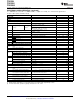


ELECTRICAL CHARACTERISTICS
TPS65053
TPS650531
TPS650532
www.ti.com
............................................................................................................................................. SLVS754C – MARCH 2007 – REVISED SEPTEMBER 2009
RECOMMENDED OPERATING CONDITIONS (continued)
MIN NOM MAX UNIT
I
LDO2,3
Output current at VLDO2,3 200 mA
T
A
Operating ambient temperature range – 40 85 ° C
T
J
Operating junction temperature range – 40 125 ° C
R
CC
Resistor from battery voltage to V
CC
used for filtering
(2)
1 10 Ω
(2) Up to 2 mA can flow into V
CC
when both converters are running in PWM, this resistor causes the UVLO threshold to be shifted
accordingly.
V
cc
= VINDCDC1/2 = 3.6V, EN = V
cc
, MODE = GND, L = 2.2 µ H, C
OUT
= 22 µ F, T
A
= – 40 ° C to 85 ° C typical values
are at T
A
= 25 ° C (unless otherwise noted).
PARAMETER TEST CONDITIONS MIN TYP MAX UNIT
SUPPLY CURRENT
V
cc
Input voltage range 2.5 6 V
One converter, I
OUT
= 0 mA.PFM mode enabled
(Mode = GND) device not switching,
20 30 µ A
EN_DCDC1 = Vin OR EN_DCDC2 = Vin;
EN_LDO1= EN_LDO2 = EN_LDO3 = GND
Two converters, I
OUT
= 0 mA, PFM mode enabled
Operating quiescent current
(Mode = 0) device not switching,
I
Q
Total current into V
CC
, VINDCDC1/2, 32 40 µ A
EN_DCDC1 = Vin AND EN_DCDC2 = Vin;
VINLDO1, VINLDO2/3
EN_LDO1 = EN_LDO2 = EN_LDO3 = GND
One converter, I
OUT
= 0 mA, PFM mode enabled
(Mode = GND) device not switching,
145 210 µ A
EN_DCDC1 = Vin OR EN_DCDC2 = Vin;
EN_LDO1 = EN_LDO2 = EN_LDO3 = Vin
One converter, I
OUT
= 0 mA, Switching with no load
(Mode = Vin), PWM operation
0.85 mA
EN_DCDC1 = Vin OR EN_DCDC2 = Vin;
EN_LDO1 = EN_LDO2 = EN_LDO3 = GND
I
Q
Operating quiescent current into V
CC
Two converters, I
OUT
= 0 mA, Switching with no load
(Mode = Vin), PWM operation
1.25 mA
EN_DCDC1 = Vin AND EN_DCDC2 = Vin;
EN_LDO1 = EN_LDO2 = EN_LDO3 = GND
EN_DCDC1 = EN_DCDC2 = GND
I
(SD)
Shutdown current 9 12 µ A
EN_LDO1 = EN_LDO2 = EN_LDO3 = GND
Undervoltage lockout threshold for DCDC
UVLO Voltage at V
CC
1.8 2 V
converters and LDOs
EN_DCDC1, EN_DCDC2, EN_LDO1, EN_LDO2, EN_LDO3, MODE
MODE, EN_DCDC1, EN_DCDC2, EN_LDO1, EN_LDO2,
V
IH
High-level input voltage 1.2 V
CC
V
EN_LDO3
MODE, EN_DCDC1, EN_DCDC2, EN_LDO1, EN_LDO2,
V
IL
Low-level input voltage 0 0.4 V
EN_LDO3
MODE, EN_DCDC1, EN_DCDC2, EN_LDO1, EN_LDO2,
I
IN
Input bias current 0.01 1 µ A
EN_LDO3, MODE = GND or VIN
POWER SWITCH
VINDCDC1/2 = 3.6 V 280 630
P-channel MOSFET on DCDC1,
r
DS(on)
m Ω
resistance DCDC2
VINDCDC1/2 = 2.5 V 400
I
LD_PMOS
P-channel leakage current V
(DS)
= 6 V 1 µ A
VINDCDC1/2 = 3.6 V 220 450
N-channel MOSFET on DCDC1,
r
DS(on)
m Ω
resistance DCDC2
VINDCDC1/2 = 2.5 V 320
I
LK_NMOS
N-channel leakage current V
(DS)
= 6 V 7 10 µ A
DCDC1 1.19 1.4 1.65
DCDC2
Forward Current Limit 0.85 1 1.15
(TPS65053)
I
(LIMF)
PMOS (High-Side) and 2.5 V ≤ V
IN
≤ 6 V A
NMOS (Low side)
DCDC2
(TPS650531, 1.19 1.4 1.65
TPS650532)
T
SD
Thermal shutdown Increasing junction temperature 150 ° C
Thermal shutdown hysteresis Decreasing junction temperature 20 ° C
Copyright © 2007 – 2009, Texas Instruments Incorporated Submit Documentation Feedback 3
Product Folder Link(s): TPS65053 TPS650531 TPS650532