
Datasheet


ENABLE
LDO1
LDO2
DETAILED DESCRIPTION
STEP-DOWN CONVERTERS, VDCDC1, VDCDC2 AND VDCDC3
TPS650240 , , TPS650241
TPS650242 , TPS650243
TPS650244 , TPS650245
www.ti.com
.............................................................................................................................................................. SLVS774B – JUNE 2007 – REVISED JULY 2009
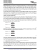
STARTUP LDO1 AND LDO2
Figure 17.
The TPS65024x incorporate three synchronous step-down converters operating typically at 2.25MHz fixed
frequency PWM (Pulse Width Modulation) at moderate to heavy load currents. At light load currents the
converters automatically enter Power Save Mode and operate with PFM (Pulse Frequency Modulation).
VDCDC1 delivers up to 1.6A, VDCDC2 is capable of delivering up to 1.0A of output current while the VDCDC3
converter is capable of delivering up to 800mA.
The converter output voltages can be programmed via the DEFDCDC1, DEFDCDC2 and DEFDCDC3 pins. The
pins can either be connected to GND, VCC or to a resistor divider between the output voltage and GND. The
VDCDC1 converter defaults to 2.80V or 3.3V depending on the DEFDCDC1 configuration pin, if DEFDCDC1 is
tied to ground the default is 2.80V, if it is tied to VCC the default is 3.3V. When the DEFDCDC1 pin is connected
to a resistor divider, the output voltage can be set in the range of 0.6V to VINDCDC1 V. Reference the section
on Output Voltage Selection for details on setting the output voltage range.
The VDCDC2 converter defaults to 1.8V or 2.5V depending on the DEFDCDC2 configuration pin, if DEFDCDC2
is tied to ground the default is 1.8V, if it is tied to VCC the default is 2.5V. When the DEFDCDC2 pin is
connected to a resistor divider, the output voltage can be set in the range of 0.6V to VINDCDC2 V.
The VDCDC3 converter defaults to 1.0V or 1.3V for the TPS650240 depending on the DEFDCDC3 configuration
pin, if DEFDCDC3 is tied to ground the default is 1.0V, if it is tied to VCC the default is 1.3V. The DEFDCDC3
pin cannot be connected to a resistor divider. In opposition to DEFDCDC1 and DEFDCDC2, the DEFDCDC3 pin
can be used to change the core voltage during operation by changing its logic level from HIGH to LOW or vice
versa. TPS650241 to TPS650245 allow different voltages for the VDCDC3 converter. Reference Table 4 for the
TPS650240, TPS650241, TPS650242, TPS650243, TPS650244 and TPS650245 default voltage options.
Copyright © 2007 – 2009, Texas Instruments Incorporated Submit Documentation Feedback 17
Product Folder Link(s): TPS650240 TPS650241 TPS650242 TPS650243 TPS650244 TPS650245