
Datasheet


SLVS485 − AUGUST 2003
www.ti.com
2
These devices have limited built-in ESD protection. The leads should be shorted together or the device placed in conductive foam during
storage or handling to prevent electrostatic damage to the MOS gates.
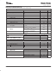
ORDERING INFORMATION
PLASTIC SOT23-6
(1)
(2)
(DBV)
OUTPUT VOLTAGE MINIMUM ON-TIME MINIMUM OFF-TIME MARKING
TPS64200DBVR
Adjustable
1.2 V to V
I
ON time = 1.6 µs OFF time = 600 ns PJAI
TPS64201DBVR
Adjustable
1.2 V to V
I
Variable minimum on time OFF time = 600 ns PJBI
TPS64202DBVR
Adjustable
1.2 V to V
I
Variable minimum on time OFF time = 300 ns PJCI
TPS64203DBVR
Adjustable
1.2 V to V
I
ON time = 600 ns OFF time = 600 ns PJDI
(1)
The R suffix indicates shipment in tape and reel with 3000 units per reel.
(2)
The T suffix indicates a mini reel with 250 units per reel.
ABSOLUTE MAXIMUM RATINGS
over operating free-air temperature range unless otherwise noted
(1)
Supply voltage, VIN −0.3 V to 7 V
Voltage at EN, SW, ISENSE −0.3 V to VIN
Voltage at FB −0.3 V to 3.3 V
Maximum junction temperature, T
J
150°C
Operating free−air temperature, T
A
−40°C to 85°C
Storage temperature, T
sgt
−65°C to 150°C
Lead temperature 1,6 mm (1/16 inch) from case for 10 seconds 300°C
(1)
Stresses beyond those listed under “absolute maximum ratings” may cause permanent damage to the device. These are stress ratings only, and
functional operation of the device at these or any other conditions beyond those indicated under “recommended operating conditions” is not
implied. Exposure to absolute-maximum-rated conditions for extended periods may affect device reliability.
PACKAGE DISSIPATION RATINGS
PACKAGE
T
A
≤255C
POWER RATING
DERATING FACTOR
ABOVE T
A
= 25°C
T
A
= 705C
POWER RATING
T
A
= 855C
POWER RATING
SOT23−6 400 mW 4 mW/°C 220 mW 180 mW
NOTE
:
The thermal resistance junction to ambient of the 6−pin SOT23 package is 250°C/W.
RECOMMENDED OPERATING CONDITIONS
MIN NOM MAX UNIT
Supply voltage at VIN 1.8 6.5 V
Operating junction temperature −40 125 °C