
Datasheet


www.ti.com
Bit Decoding
Acknowledge
MODE Selection
TPS62410
SLVS737 – FEBRUARY 2007
DETAILED DESCRIPTION (continued)
The Interface is activated if at least one of the converters is enabled (EN1 or EN2 is high). After the Startup-time
t
Start
(170 µ s) the interface is ready for data reception.
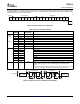
Table 1. Addressable Registers for Adjustable Output Voltage Devices
REGISTER DESCRIPTION A1 A0 D4 D3 D2 D1 D0
REG_DEF_1_High Not available in TPS62410 adjustable version 0 1
REG_DEF_1_Low Converter 1 output voltage setting 0 0 TPS62410 see Table 3
REG_DEF_2 Converter 2 output voltage 1 0 TPS62410 see Table 4 , connect ADJ2
pin directly to VOUT
2
Don’t use 1 1
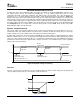
The bit detection is based on a PWM scheme, where the criterion is the relation between t
LOW
and t
HIGH
. It can
be simplified to:
High Bit: t
High
> t
Low
, but with t
High
at least 2x t
Low
, see Figure 30
Low Bit: tLow> tHigh, but with tLow at least 2x tHigh, see Figure 30
The bit detection starts with a falling edge on the MODED/DATA pin and ends with the next falling edge.
Depending on the relation between t
Low
and t
High
a 0 or 1 is detected.
The Acknowledge condition is only applied if:
• Acknowledge is requested by a set RFA bit
• The transmitted device address matches with the device address of the device
• 16 bits were received correctly
In this case, the device turns on the internal ACKN-MOSFET and pulls the MODE/DATA pin low for the time
tACKN, which is max. 520 µ s. The Acknowledge condition is valid after an internal delay time t
valACK
. This means
the internal ACKN-MOSFET is turned on after t
valACK
, when the last falling edge of the protocol was detected.
The master controller keeps the line low during this time.
The master device can detect the acknowledge condition with it’s input by releasing the MODE/DATA pin after
tvalACK and read back a 0.
In case of an invalid device address or not correctly received protocol, no acknowledge condition will be applied,
thus the internal MOSFET will not be turned on and the external pullup resistor pulls MODE/DATA pin high after
t
valACK
. The MODE/DATA pin can be used again after the acknowledge condition ends.
NOTE:
The acknowledge condition may only be requested in case the master device has an
open drain output.
In case of a push pull output stage it is recommended to use a series resistor in the MODE/DATA line to limit the
current to 500 µ A in case of an accidentally requested acknowledge to protect the internal ACKN-MOSFET.
Because of the MODE/DATA pin is used for two functions, interface and a MODE selection, the device needs to
determine when it has to decode the bit stream or to change the operation mode.
The device enters forced PWM mode operation immediately whenever the MODE/DATA pin turns to high level.
The device stays also in forced PWM mode during the whole time of a protocol reception.
With a falling edge on the MODE/DATA pin the device starts bit decoding. If the MODE/DATA pin stays low for
at least t
timeout
, the device get’s an internal timeout and Power Save Mode operation is enabled.
18
Submit Documentation Feedback