
Datasheet


GateDriver
Anti
Shoot-Through
Current
LimitComparator
SW
Softstart
Bandgap
Undervoltage
Lockout
Limit
HighSide
Limit
LowSide
FB
EN
MODE
VIN
GND
Min.On Time
Min.OFF Time
VIN
EN
Integrated
FeedBack
Network
VREF
FB
Error
Comparator
Zero/Negative
CurrentLimitComparator
Control
Logic
PMOS
NMOS
MODE
Thermal
Shutdown
VREF
0.70V
1
2
3
6
5
4
MODE
SW
VIN
FB
EN
GND
DRY PACKAGE
(TOP VIEW)
TPS62230, TPS62231, TPS62232, TPS62233, TPS62234, TPS62235, TPS62236
TPS62237, TPS62238, TPS62239, TPS622310, TPS622311, TPS622312
TPS622313, TPS622314, TPS622315, TPS622316, TPS622317, TPS622318
www.ti.com
SLVS941E –APRIL 2009–REVISED DECEMBER 2010
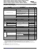
PIN FUNCTIONS
PIN
I/O DESCRIPTION
NAME NO
VIN 3 PWR V
IN
power supply pin.
GND 4 PWR GND supply pin
EN 5 IN This is the enable pin of the device. Pulling this pin to low forces the device into shutdown mode. Pulling
this pin to high enables the device. This pin must be terminated.
SW 2 OUT This is the switch pin and is connected to the internal MOSFET switches. Connect the inductor to this
terminal
FB 6 IN Feedback Pin for the internal regulation loop. Connect this pin directly to the output capacitor.
MODE 1 IN MODE pin = high forces the device to operate in PWM mode. Mode = low enables the Power Save Mode
with automatic transition from PFM (Pulse frequency mode) to PWM (pulse width modulation) mode.
FUNCTIONAL BLOCK DIAGRAM
Copyright © 2009–2010, Texas Instruments Incorporated Submit Documentation Feedback 5