
Datasheet


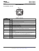


16 15 14 13
5 6 7 8
1
2
3
4 9
GND
GND
FB
AGND
PGND
Exposed
Thermal
Pad
VIN
VIN
EN
PGND
SW
LBI
VINA
SW
PG
SYNC
LBO
12
11
10
TPS62110, TPS62111
TPS62112, TPS62113
www.ti.com
SLVS585C –JULY 2005–REVISED OCTOBER 2012
DEVICE INFORMATION
PIN ASSIGNMENT TOP VIEW
TERMINAL FUNCTIONS
TERMINAL
I/O DESCRIPTION
NAME NO.
AGND 9 I Analog ground, connect to GND and PGND
Enable. A logic high enables the converter; logic low forces the device into shutdown mode reducing the
EN 4 I
supply current to less than 2 µA. Do not leave floating.
Feedback pin for the fixed output voltage versions. Connect to V
OUT
for these devices. For the
FB 10 I adjustable versions, an external resistive divider is connected to this pin. The internal voltage divider is
disabled for the adjustable versions.
GND 11, 12 I Ground
LBI 7 I Low-battery input. Do not leave floating.
Open-drain, low-battery output. This pin is pulled low if LBI is below its threshold. If not used, the pin
LBO 6 O
may be left floating or connected to GND.
Power good comparator output. This is an open-drain output. A pullup resistor should be connected
PG 13 O between PG and VOUT. The output goes high when the output voltage is greater than 98.4% of the
nominal value. If not used, the pin may be left floating or connected to GND.
PGND 1, 16 I Power ground. Connect all power grounds to this pin.
Connect the inductor to this pin. This pin is the switch pin and connected to the drain of the internal
SW 14, 15 O
power MOSFETS.
Input for synchronization to external clock signal. Synchronizes the converter switching frequency to an
external clock signal with CMOS level. Also controls power save mode by being tied high or low:
SYNC 5 I
SYNC = HIGH: Low-noise mode enabled, fixed frequency PWM operation is forced
SYNC = LOW (GND): Power save mode enabled, PFM/PWM Mode enabled
VIN 2, 3 I Supply voltage input (power stage)
VINA 8 I Supply voltage input (support circuits)
Exposed Connect to AGND. Must be soldered to achieve appropriate power dissipation and mechanical
Thermal pad reliability.
Copyright © 2005–2012, Texas Instruments Incorporated Submit Documentation Feedback 5
Product Folder Links: TPS62110 TPS62111 TPS62112 TPS62113