
Datasheet


TPS61200
TPS61201
TPS61202
SLVS577D –MARCH 2007–REVISED MARCH 2013
www.ti.com
These devices have limited built-in ESD protection. The leads should be shorted together or the device placed in conductive foam
during storage or handling to prevent electrostatic damage to the MOS gates.
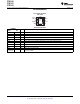
AVAILABLE DEVICE OPTIONS
(1)
PACKAGE
T
A
OUTPUT VOLTAGE PACKAGE
(2)
PART NUMBER
(3)
MARKING
Adjustable BRR TPS61200DRC
3.3 V BRS 10-Pin SON, 1 mm height TPS61201DRC
–40°C to 85°C
5 V BRT TPS61202DRC
5 V CER 10-Pin SON, 0.8 mm height TPS61202DSC
(1) Contact the factory to check availability of other fixed output voltage versions.
(2) For the most current package and ordering information, see the Package Option Addendum at the end of this document, or see the TI
website at www.ti.com.
(3) The DRC and the DSC package are available taped and reeled. Add R suffix to device type (e.g., TPS61200DRCR or TPS61202DSCR)
to order quantities of 3000 devices per reel. It is also available in minireels. Add a T suffix to the device type (i.e. TPS61200DRCT or
TPS61202DSCT) to order quantities of 250 devices per reel.
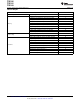
ABSOLUTE MAXIMUM RATINGS
over operating free-air temperature range (unless otherwise noted)
(1)
TPS6120x UNIT
V
IN
Input voltage range on VIN, L, VAUX, VOUT, PS, EN, FB, UVLO – 0.3 to 7 V
T
J
Operating junction temperature range –40 to 150 °C
T
stg
Storage temperature range –65 to 150 °C
Human Body Model (HBM)
(2)
4 kV
ESD Machine Model (MM)
(2)
200 V
Charged Device Model (CDM)
(2)
1.5 kV
(1) Stresses beyond those listed under Absolute Maximum Ratings may cause permanent damage to the device. These are stress ratings
only, and functional operation of the device at these or any other conditions beyond those indicated under Recommended Operating
Conditions is not implied. Exposure to absolute-maximum-rated conditions for extended periods may affect device reliability.
(2) ESD testing is performed according to the respective JESD22 JEDEC standard.
THERMAL INFORMATION
DRC DSC
THERMAL METRIC
(1)
UNITS
10 PINS 10 PINS
θ
JA
Junction-to-ambient thermal resistance 41.2 40.4
θ
JCtop
Junction-to-case (top) thermal resistance 62.8 37.8
θ
JB
Junction-to-board thermal resistance 16.6 15.4
°C/W
ψ
JT
Junction-to-top characterization parameter 1.2 0.3
ψ
JB
Junction-to-board characterization parameter 16.8 15.6
θ
JCbot
Junction-to-case (bottom) thermal resistance 4.1 2.8
(1) For more information about traditional and new thermal metrics, see the IC Package Thermal Metrics application report, SPRA953.
RECOMMENDED OPERATING CONDITIONS
MIN NOM MAX UNIT
V
IN
Input voltage at VIN 0.3 5.5 V
T
A
Operating free air temperature range –40 85 °C
T
J
Operating junction temperature range –40 125 °C
2 Submit Documentation Feedback Copyright © 2007–2013, Texas Instruments Incorporated
Product Folder Links: TPS61200 TPS61201 TPS61202