
Datasheet


P1
1
f =
2 x 6 M x C3p W
P2
2
f =
2 x Rout x C2p
2
RHPZ
Rout
f = x
2 x L
Vin
Voutp
æ ö
ç ÷
è ø
Z
1
f =
2 x R3 x C3p
1.229
A =
Vout
Vin 1
x Gea x 6 M x x Rout x
Vout x Rsense 2
W
C
out
+
ǒ
V
out
* V
in
Ǔ
I
out
V
out
Fs V
ripple
V
ripple_ESR
+ I
out
R
ESR
TPS61170
www.ti.com
SLVS789C – NOVEMBER 2007– REVISED APRIL 2011
COMPENSATION CAPACITOR SELECTION
The TPS61170 has an external compensation, COMP pin, which allows the loop response to be optimized for
each application. The COMP pin is the output of the internal error amplifier. An external resistor R3 and ceramic
capacitor C3 are connected to COMP pin to provide a pole and a zero. This pole and zero, along with the
inherent pole of a current mode control boost converter, determine the close loop frequency response. This is
important to a converter stability and transient response.
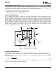
The following equations summarize the poles, zeros and DC gain of a TPS61170 boost converter with ceramic
output capacitor (C2), as shown in the block diagram. They include the dominant pole (f
P1
), the output pole (f
P2
)
of a boost converter, the right-half-plane zero (f
RHPZ
) of a boost converter, the zero (f
Z
) generated by R3 and C3,
and the DC gain (A).
(7)
(8)
(9)
(10)
(11)
where Rout is the load resistance, Gea is the error amplifier transconductance located in the ELECTRICAL
CHARACTERISTICS table, Rsense (100mΩ typical) is a sense resistor in the current control loop. These
equations helps generate a simple bode plot for TPS61170 loop analysis.
Increasing R3 or reducing C3 increases the close loop bandwidth which improves the transient response.
Adjusting R3 and C3 in opposite directions increase the phase, and help loop stability. For many of the
applications, the recommended value of 10k and 680pF makes an ideal compromise between transient response
and loop stability. To optimize the compensation, use C3 in the range of 100pF to 10nF, and R3 of 10k. See the
TI application report SLVA319 for thorough analysis and description of the boost converter small signal model
and compensation design.
INPUT AND OUTPUT CAPACITOR SELECTION
The output capacitor is mainly selected to meet the requirements for the output ripple and loop stability. The
ripple voltage is related to the capacitor’s capacitance and its equivalent series resistance (ESR). Assuming a
capacitor with zero ESR, the minimum capacitance needed for a given ripple can be calculated using
Equation 12.
(12)
Where, V
ripple
= peak-to-peak output ripple. The additional output ripple component caused by ESR is calculated
using:
(13)
Due to its low ESR, Vripple_ESR can be neglected for ceramic capacitors, but must be considered if tantalum or
electrolytic capacitors are used.
Care must be taken when evaluating a ceramic capacitor’s derating under dc bias, aging and AC signal. For
example, larger form factor capacitors (in 1206 size) have a resonant frequencies in the range of the switching
frequency. So, the effective capacitance is significantly lower. The DC bias can also significantly reduce
capacitance. Ceramic capacitors can lose as much as 50% of its capacitance at its rated voltage. Therefore,
choose a ceramic capacitor with a voltage rating at least 1.5X its expected dc bias voltage.
Copyright © 2007–2011, Texas Instruments Incorporated 17