
Datasheet


CTRL
low
high
FB
200mVxdutycycle
Insertbattery
CTRL
low
high
FB
Insertbattery
Programming
code
FBramp
Shutdowndelay
t
EnterESmode
Timingwindow
Programmingcode
50mV 50mV
EnterESmode
PWMsignal
Startup
delay
PWM
mode
Startupdelay
FBramp
Programmedvalue
(ifnotprogrammed, 200mVdefault)
Shutdown
delay
IC
Shutdown
Startupdelay
FBramp
ES
mode
ESdetectdelay
ESdetecttime
V
FB
+ Duty 1.229 V
TPS61170
SLVS789C – NOVEMBER 2007– REVISED APRIL 2011
www.ti.com
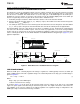
FEEDBACK REFERENCE PROGRAM MODE SELECTION
The CTRL pin is used for changing the FB pin reference voltage on-the-fly. There are two methods to program
the reference voltage, PWM signal and 1 wire interface (EasyScale™). The programming mode is selected each
time the device is enabled. The default mode is to use the duty cycle of the PWM signal on the CTRL pin to
modulate the reference voltage. To enter the 1 wire interface mode, the following digital pattern on the CTRL pin
must be recognized by the IC every time the IC starts from the shutdown mode.
1. Pull CTRL pin high to enable the TPS61170 and to start the 1 wire mode detection window.
2. After the EasyScale detection delay (t
es_delay
, 100μsec) expires, drive CTRL low for more than the EasyScale
detection time (t
es_detect
, 260μsec).
3. The CTRL pin has to be low for more than EasyScale detection time before the EasyScale detection window
(t
es_win
, 1msec) expires. EasyScale detection window starts from the first CTRL pin low to high transition.
The IC immediately enters the 1 wire mode once the above 3 conditions are met. The EasyScale communication
can start before the detection window expires. Once the mode is programmed, it can not be changed without
another start up. In other words, the IC must be shutdown by pulling the CTRL low for 2.5ms and restarted in
order to exit EasyScale Mode. See the Mode Detection of Feedback Reference Program figure (Figure 13) for a
graphical explanation.
Figure 13. Mode Detection of Feedback Reference Program
PWM PROGRAM MODE
When the CTRL pin is constantly high, the FB voltage is regulated to 1.229V typically. However, the CTRL pin
allows a PWM signal to lower this regulation voltage. The relationship between the duty cycle and FB voltage is
given in Equation 1:
(1)
Where:
Duty = duty cycle of the PWM signal
1.229 V = internal reference voltage
As shown in Figure 14, the IC chops up the internal 1.229V reference voltage at the duty cycle of the PWM
signal. The pulse signal is then filtered by an internal low pass filter. The output of the filter is connected to the
error amplifier as the reference voltage for the FB pin regulation. The regulation voltage is independent of the
PWM logic voltage level which often has large variations.
10 Copyright © 2007–2011, Texas Instruments Incorporated