
Datasheet


www.ti.com
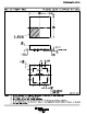
THERMAL INFORMATION
P
D(MAX)
+
T
J(MAX)
* T
A
R
qJA
+
150°C * 85°C
155°CńW
+ 420 mW
(11)
TPS61130
TPS61131
TPS61132
SLVS431B – JUNE 2002 – REVISED JANUARY 2008
Implementation of integrated circuits in low-profile and fine-pitch surface-mount packages typically requires
special attention to power dissipation. Many system-dependent issues such as thermal coupling, airflow, added
heat sinks and convection surfaces, and the presence of other heat-generating components affect the
power-dissipation limits of a given component.
Three basic approaches for enhancing thermal performance are listed below.
• Improving the power dissipation capability of the PCB design.
• Improving the thermal coupling of the component to the PCB.
• Introducing airflow in the system.
The maximum recommended junction temperature (T
J
) of the TPS6113x devices is 150 ° C. The thermal
resistance of the 16-pin TSSOP package (PW) is R
Θ JA
= 155 ° C/W. The 16-pin QFN PowerPAD package (RSA)
has a thermal resistance of R
Θ JA
= 38.1 ° C/W, if the PowerPAD is soldered and the board layout is optimized.
Specified regulator operation is assured to a maximum ambient temperature T
A
of 85 ° C. Therefore, the
maximum power dissipation is about 420 mW for the TSSOP (PW) package and 1700 mW for the QFN (RSA)
package. More power can be dissipated if the maximum ambient temperature of the application is lower (see
Equation 11 ).
If designing for a lower junction temperature of 125 ° C, which is recommended, maximum heat dissipation is
lower. Using the above Equation 11 results in 1050 mW power dissipation for the RSA package and 260 mW for
the PW package.
22 Submit Documentation Feedback Copyright © 2002 – 2008, Texas Instruments Incorporated
Product Folder Link(s): TPS61130 TPS61131 TPS61132