
Datasheet


COMP
FB
GM Amplifier
Vref
SW SW
GateDriverof
Power
Transistor
IN
SS
PWM
Generator
Currentlimit
and
SoftStart
t Generator
OFF
t
ON
PGND
BiasVref = 1 .238V
UVLO
ThermalShutdown
AGND
EN
FREQ
V
IN
V
S
TPS61087
SLVS821C –MAY 2008–REVISED JULY 2013
www.ti.com
DETAILED DESCRIPTION
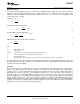
Figure 13. Block Diagram
The boost converter is designed for output voltages up to 18.5 V with a switch peak current limit of 3.2 A
minimum. The device, which operates in a current mode scheme with quasi-constant frequency, is externally
compensated for maximum flexibility and stability. The switching frequency is selectable between 650 kHz and
1.2 MHz and the minimum input voltage is 2.5 V. To limit the inrush current at start-up a soft-start pin is
available.
TPS61087 boost converter’s novel topology using adaptive off-time provides superior load and line transient
responses and operates also over a wider range of applications than conventional converters.
The selectable switching frequency offers the possibility to optimize the design either for the use of small sized
components (1.2 MHz) or for higher system efficiency (650 kHz). However, the frequency changes slightly
because the voltage drop across the r
DS(on)
has some influence on the current and voltage measurement and
thus on the on-time (the off-time remains constant).
The converter operates in continuous conduction mode (CCM) as soon as the input current increases above half
the ripple current in the inductor, for lower load currents it switches into discontinuous conduction mode (DCM). If
the load is further reduced, the part starts to skip pulses to maintain the output voltage.
8 Submit Documentation Feedback Copyright © 2008–2013, Texas Instruments Incorporated
Product Folder Links: TPS61087