
Datasheet


www.ti.com
DESIGN PROCEDURE
Programming the TPS61010 Adjustable Output Voltage Device
R3 R4
V
O
V
FB
–1
500 k
V
O
500 mV
–1
(1)
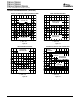
VBAT
LBI
EN
ADEN
VOUT
LBO
FB
COMP
SW
GND
C
IN
10 µF
10 V
L1
10 µH
R5
C
OUT
22 µF
10 V
C
C1
10 pF
C
C2
10 nF
R
C
6
9
1
8
4
2
3
10
5
7
VOUT = 3.3 V
Low Battery Warning
TPS61016
1 Cell
NiMH,
NiCd or
Alkaline
R1
R2
R3
100 kΩ
R4
programming the low battery comparator threshold voltage
TPS61010, TPS61011
TPS61012, TPS61013
TPS61014, TPS61015, TPS61016
SLVS314D – SEPTEMBER 2000 – REVISED JUNE 2005
The TPS6101x boost converter family is intended for systems that are powered by a single-cell NiCd or NiMH
battery with a typical terminal voltage between 0.9 V to 1.6 V. It can also be used in systems that are powered by
two-cell NiCd or NiMH batteries with a typical stack voltage between 1.8 V and 3.2 V. Additionally, single- or
dual-cell, primary and secondary alkaline battery cells can be the power source in systems where the TPS6101x
is used.
The output voltage of the TPS61010 can be adjusted with an external resistor divider. The typical value of the
voltage on the FB pin is 500 mV in fixed frequency operation and 485 mV in the power-save operation mode.
The maximum allowed value for the output voltage is 3.3 V. The current through the resistive divider should be
about 100 times greater than the current into the FB pin. The typical current into the FB pin is 0.01 µA, and the
voltage across R4 is typically 500 mV. Based on those two values, the recommended value for R4 is in the range
of 500 k Ω in order to set the divider current at 1 µA. From that, the value of resistor R3, depending on the
needed output voltage (V
O
), can be calculated using Equation 1 .
If, as an example, an output voltage of 2.5 V is needed, a 2-M Ω resistor should be chosen for R3.
Figure 22. Typical Application Circuit for Adjustable Output Voltage Option
The output voltage of the adjustable output voltage version changes with the output current. Due to
device-internal ground shift, which is caused by the high switch current, the internal reference voltage and the
voltage on the FB pin increases with increasing output current. Since the output voltage follows the voltage on
the FB pin, the output voltage rises as well with a rate of 1 mV per 1-mA output current increase. Additionally,
when the converter goes into pulse-skip mode at output currents around 5 mA and lower, the output voltage
drops due to the hysteresis of the controller. This hysteresis is about 15 mV, measured on the FB pin.
The current through the resistive divider should be about 100 times greater than the current into the LBI pin. The
typical current into the LBI pin is 0.01 µA, the voltage across R2 is equal to the reference voltage that is
generated on-chip, which has a value of 500 mV ± 15 mV. The recommended value for R2 is therefore in the
range of 500 k Ω . From that, the value of resistor R1, depending on the desired minimum battery voltage V
BAT
,
can be calculated using Equation 2 .
15