
Datasheet


SLVS391B − OCTOBER 2001 − REVISED FEBRUARY 2002
2
www.ti.com
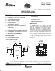
pin assignments
1
2
3
4
5
10
9
8
7
6
EN
PG
C2F−
C2F+
VIN
FB
GND
C1F−
OUT
C1F+
DGS PACKAGES
(TOP VIEW)
ACTUAL SIZE
3,05 mm x 4,98 mm
AVAILABLE OPTIONS
PART NUMBER
†
MARKING DGS
PACKAGE
OUTPUT VOLTAGE
[V]
MINIMUM INPUT VOLTAGE
FOR I
O
= 150 mA
TPS60500DGS AVB
Adjustable
(0.8 V to 3.3 V)
V
I
> V
O
+ 1
TPS60501DGS AVC 3.3 V
I
> 4.3 V
TPS60502DGS AVD 1.8 V
I
> 2.8 V
TPS60503DGS AVE 1.5 V
I
> 2.5 V
†
The DGS package is available taped and reeled. Add R suffix to device type (e.g. TPS60500DGSR) to order
quantities of 2500 devices per reel.
Terminal Functions
TERMINAL
I/O
DESCRIPTION
NAME NO.
I/O
DESCRIPTION
C1F+ 6 Positive terminal of the flying capacitor C1F
C1F− 8 Negative terminal of the flying capacitor C1F
C2F+ 4 Positive terminal of the flying capacitor C2F
C2F− 3 Negative terminal of the flying capacitor C2F
EN 1 I Device-enable Input.
− EN
= High disables the device. Output and input are isolated in shutdown mode.
− EN
= Low enables the device.
GND 9 Ground
FB 10 O TPS60500: connect via voltage divider to V
O
TPS60501 to TPS60503: connect directly to V
O
OUT 7 O Regulated 3.3 V, 1.8 V, 1.5 V, or adjustable power output
Bypass OUT to GND with the output filter capacitor C
o
.
PG 2 O Open drain power good detector output. As soon as the voltage on OUT reaches about 97% of its nominal value this
pin goes high.
VIN 5 I Supply Input. Connect to an input supply in the 1.8-V to 6.5-V range.