
Datasheet


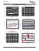


PWRGD
BOOT
PH
RT/CLK
EN
AGND
VIN
VSENSE
COMP
15 14 13
GND
12
11
10
9
8
765
16
GND
VIN
VIN
PH
PH
1
2
3
4
SS/TR
PowerPAD
(17)
QFN16
RTE PACKAGE
(TOP VIEW)
TPS57112-Q1
SLVSAL8 –DECEMBER 2010
www.ti.com
DEVICE INFORMATION
PIN CONFIGURATION
PIN FUNCTIONS
PIN
DESCRIPTION
NAME NO.
AGND 5 Analog Ground should be electrically connected to GND close to the device.
BOOT 13 A bootstrap capacitor is required between BOOT and PH. If the voltage on this capacitor is below the minimum
required by the BOOT UVLO, the output is forced to switch off until the capacitor is refreshed.
COMP 7 Error amplifier output, and input to the output switch current comparator. Connect frequency compensation
components to this pin.
EN 15 Enable pin, internal pull-up current source. Pull below 1.2 V to disable. Float to enable. Can be used to set the
on/off threshold (adjust UVLO) with two additional resistors.
GND 3, 4 Power Ground. This pin should be electrically connected directly to the power pad under the IC.
PH 10, 11, The source of the internal high side power MOSFET, and drain of the internal low side (synchronous) rectifier
12 MOSFET.
PowerPAD 17 GND pin should be connected to the exposed power pad for proper operation. This power pad should be
™ connected to any internal PCB ground plane using multiple vias for good thermal performance.
PWRGD 14 An open drain output; asserts low if output voltage is low due to thermal shutdown, overcurrent,
over/under-voltage or EN shut down.
RT/CLK 8 Resistor Timing or External Clock input pin.
SS/TR 9 Slow start and tracking. An external capacitor connected to this pin sets the output voltage rise time.
This pin can also be used for tracking.
VIN 1, 2, 16 Input supply voltage, 2.95 V to 6 V.
VSENSE 6 Inverting node of the transconductance (gm) error amplifier.
6 Submit Documentation Feedback Copyright © 2010, Texas Instruments Incorporated
Product Folder Link(s): TPS57112-Q1