
Datasheet


UVLO
Adjust
Resistors
Slow Start
Capacitor
Frequency Set
Resistor
COMP
Network
Resistor
Divider
V
PRI
VIN
Topside
Ground
Area
Via to Ground Plane
FAULT
SS
VIN
COMP
GND
VIN
GND
GND
PH
PH
EN
BOO T
VIN
VSENSE
Thermal
Pad
RT/CLK
PH
Secondary
Side Diode
Isolation
Transformer
Output
Capacitor
Primary
Capacitor
VOUT
GND
PH
Input
Bypass
Capacitor
Y Capacitor
TPS55010
www.ti.com
SLVSAV0A –APRIL 2011–REVISED JUNE 2011
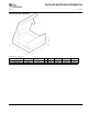
PCB LAYOUT
Layout is a critical portion of good power supply design. There are several signal paths that conduct fast
changing currents or voltages that can interact with stray inductance or parasitic capacitance to generate noise
or degrade the power supplies performance. Care should be taken to minimize the loop area formed by the
bypass capacitor connections and the VIN pins. See Figure 57 for a PCB layout example. The GND pins should
be tied directly to the thermal pad under the IC. The power pad should be connected to any internal PCB ground
planes using multiple vias directly under the IC. Additional vias can be used to connect the top side ground area
to the internal planes near the input and output capacitors.
Locate the input bypass capacitor as close to the IC as possible. The PH pin should be routed to the primary
side of the transformer. Since the PH connection is the switching node, the transformer should be located close
to the PH pins, and the area of the PCB conductor minimized to prevent excessive capacitive coupling. The boot
capacitor must also be located close to the device. The sensitive analog ground connections for the feedback
voltage divider, compensation component, slow start capacitor and frequency set resistor should be connected to
a separate analog ground trace as shown. The RT/CLK pin is particularly sensitive to noise so the R
T
resistor
should be located as close as possible to the IC and routed with minimal lengths of trace. Avoid connecting y
capacitor on nodes which experience high dv/dt.
Figure 57. PCB Layout
REVISION HISTORY
Changes from Original (April 2010) to Revision A Page
• Added production data .......................................................................................................................................................... 1
Copyright © 2011, Texas Instruments Incorporated Submit Documentation Feedback 35
Product Folder Links :TPS55010