
Datasheet


25
50
75
100
125
0 0.5 1 1.5 2 2.5 3
Pic - IC Power Dissipation - W
T = room temp
A
T - Maximum Ambient Temperature - °C
A max
3.5
25
50
75
100
125
0 0.5 1 1.5 2 2.5 3.5
Pic - IC Power Dissipation - W
T - Junction Temperature - °C
J
3
T = room temperature,
no air flow
A
0.000001
0.00001
0.0001
0.001
0.01
0.1
1
10
0.001 0.01 0.1 1 10
Track In Voltage - V
Output Voltage - V
0.000001
0.00001
0.0001
0.001
0.01
0.1
1
10
Vsense Voltage - V
Ideal Vsense
Vout
Vsense
-0.05
-0.04
-0.03
-0.02
-0.01
0
0.01
0.02
0.03
0.04
0.05
0
1
1.5
2
2.5
3 3.5
4
4.5
Output Current - A
Percent Load Regulation - %
0.5 5
Vin = 8 V
Vin = 10 V
Vin = 12 V
Vin = 15 V
Vin = 17 V
-0.05
-0.04
-0.03
-0.02
-0.01
0
0.01
0.02
0.03
0.04
0.05
8 9 10 11 12 13 14 15 16 17
Input Voltage - V
Percent Line Regulation - %
Iout = 2.5 A
Iout = 5 A
Iout = 0 A
-60
-50
-40
-30
-20
-10
0
10
20
30
40
50
60
Frequency - Hz
-180
-150
-120
-90
-60
-30
0
30
60
90
120
150
180
Gain - dB
100
1000
10000
100000
1000000
Phase - Deg
Vin = 12 V
Load = 5 A
Phase
Gain
TPS54521
www.ti.com
SLVS981C –JUNE 2010–REVISED AUGUST 2013
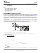
CLOSED LOOP RESPONSE LINE REGULATION
Figure 47. Figure 48.
LOAD REGULATION TRACKING PERFORMANCE
Figure 49. Figure 50.
MAXIMUM AMBIENT TEMPERATURE JUNCTION TEMPERATURE
vs vs
IC POWER DISSIPATION IC POWER DISSIPATION
Figure 51. Figure 52.
Copyright © 2010–2013, Texas Instruments Incorporated Submit Documentation Feedback 29
Product Folder Links :TPS54521