
Datasheet
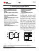


0,45
2,15
1,27
3,10
2,49
5,75
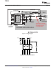
BOOT
NC
NC
VSENSE
PH
VIN
GND
ENA
Vout
PH
Vin
TOPSIDE GROUND AREA
OUTPUT
INDUCTOR
OUTPUT
FILTER
CAPACITOR
BOOT
CAPACITOR
INPUT
BYPASS
CAPACITOR
CATCH
DIODE
Route INPUT VOLTAGE
trace under the catch diode
and output capacitor
or on another layer
Signal VIA
RESISTOR
DIVIDER
Feedback Trace
EXPOSED
POWERPAD
AREA
TPS5450
SLVS757C –MARCH 2007–REVISED OCTOBER 2013
www.ti.com
Figure 9. Design Layout
spacer
Figure 10. TPS5450 Land Pattern
10 Submit Documentation Feedback Copyright © 2007–2013, Texas Instruments Incorporated
Product Folder Links: TPS5450