
Datasheet


www.ti.com
VIN
GND
C1
C10
C6
C7
C5
R2
R3
R9
R8
C16
C17
C14
C11
U1
C13
C18
C19
R5
C12
C15
C8
R6
1
C9
C4
C3
R7
R4
GND
GND
VOUT1
VOUT2
L1
L2
D1
D2
TPS54383 , , TPS54386
SLUS774B – AUGUST 2007 – REVISED OCTOBER 2007
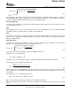
• Locate snubber components (if used) close to the rectifier diode with minimal loop area.
• Locate the BP bypass capacitor very close to the IC; a minimal loop area is recommended.
• Locate the output ceramic capacitor close to the inductor output terminal between the inductor and any
electrolytic capacitors, if used.
Figure 37. Top Layer Copper Layout and Component Placement
Copyright © 2007, Texas Instruments Incorporated Submit Documentation Feedback 31
Product Folder Link(s): TPS54383 TPS54386