
Datasheet


RT/CLK
TPS54320
Rrt
RT/CLK
modeselect
Css(nF) Vref(V)
Tss(ms) =
Iss( A)
´
m
TPS54320
SLVS982A –AUGUST 2010–REVISED SEPTEMBER 2010
www.ti.com
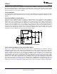
Figure 21. Works with Both RT mode and CLK mode
Slow Start (SS/TR)
The device uses the lower voltage of the internal voltage reference or the SS/TR pin voltage as the reference
voltage and regulates the output accordingly. A capacitor on the SS/TR pin to ground implements a slow start
time. The device has an internal pull-up current source of 2.3mA that charges the external slow start capacitor.
The calculations for the slow start time (Tss, 10% to 90%) and slow start capacitor (Css) are shown in
Equation 5. The voltage reference (Vref) is 0.8 V and the slow start charge current (Iss) is 2.3mA.
(5)
When the input UVLO is triggered, the EN pin is pulled below 1.21V, or a thermal shutdown event occurs the
device stops switching and enters low current operation. At the subsequent power up, when the shutdown
condition is removed, the device does not start switching until it has discharged its SS/TR pin to ground ensuring
proper soft start behavior.
Power Good (PWRGD)
The PWRGD pin is an open drain output. Once the VSENSE pin is between 94% and 106% of the internal
voltage reference the PWRGD pin pull-down is de-asserted and the pin floats. It is recommended to use a
pull-up resistor between the values of 10kΩ and 100kΩ to a voltage source that is 5.5V or less. The PWRGD is
in a defined state once the VIN input voltage is greater than 1V but with reduced current sinking capability. The
PWRGD achieves full current sinking capability once the VIN input voltage is above 4.5V.
The PWRGD pin is pulled low when VSENSE is lower than 91% or greater than 109% of the nominal internal
reference voltage. Also, the PWRGD is pulled low, if the input UVLO or thermal shutdown are asserted, the EN
pin is pulled low, or the SS/TR pin is below 1.2V typically.
Bootstrap Voltage (BOOT) and Low Dropout Operation
The device has an integrated boot regulator, and requires a small ceramic capacitor between the BOOT and PH
pins to provide the gate drive voltage for the high-side MOSFET. The boot capacitor is charged when the BOOT
pin voltage is less than VIN and BOOT-PH voltage is below regulation. The value of this ceramic capacitor
should be 0.1mF. A ceramic capacitor with an X7R or X5R grade dielectric with a voltage rating of 10V or higher
is recommended because of the stable characteristics over temperature and voltage.
To improve dropout, the device is designed to operate at 100% duty cycle as long as the BOOT to PH pin
voltage is greater than the BOOT-PH UVLO threshold which is typically 2.1V. When the voltage between BOOT
and PH drops below the BOOT-PH UVLO threshold the high-side MOSFET is turned off and the low-side
MOSFET is turned on allowing the boot capacitor to be recharged. In applications with split input voltage rails
100% duty cycle operation can be achieved as long as (VIN – PVIN) > 4V.
A boot resistor in series with the boot capacitor should never be used on the TPS54320.
14 Submit Documentation Feedback Copyright © 2010, Texas Instruments Incorporated
Product Folder Link(s) :TPS54320