
Datasheet


TPS54260-Q1
www.ti.com
SLVSAH8D –DECEMBER 2010–REVISED AUGUST 2013
APPLICATION INFORMATION
Design Guide — Step-By-Step Design Procedure
This example details the design of a high frequency switching regulator design using ceramic output capacitors.
A few parameters must be known in order to start the design process. These parameters are typically determined
at the system level. For this example, use the following known parameters:
Output Voltage 3.3 V
Transient Response 0 to 1.5A load step ΔVout = 3 %
Maximum Output Current 2.5 A
Input Voltage 12 V nom. 10.8 V to 13.2 V
Output Voltage Ripple 1% of Vout
Start Input Voltage (rising VIN) 6 V
Stop Input Voltage (falling VIN) 5.5 V
Selecting the Switching Frequency
The first step is to decide on a switching frequency for the regulator. Typically, the user chooses the highest
switching frequency possible because it produces the smallest solution size. The high switching frequency allows
for lower valued inductors and smaller output capacitors compared to a power supply that switches at a lower
frequency. The switching frequency that can be selected is limited by the minimum on-time of the internal power
switch, the input voltage and the output voltage and the frequency shift limitation.
Equation 12 and Equation 13 must be used to find the maximum switching frequency for the regulator, choose
the lower value of the two equations. Switching frequencies higher than these values result in pulse skipping or
the lack of overcurrent protection during a short circuit.
The typical minimum on time, t
onmin
, is 135 ns for the TPS54260-Q1. For this example, the output voltage is 3.3 V
and the maximum input voltage is 13.2 V, which allows for a maximum switch frequency up to 2247 kHz when
including the inductor resistance, on resistance output current and diode voltage in Equation 12. To ensure
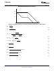
overcurrent runaway is not a concern during short circuits in your design use Equation 13 or the solid curve in
Figure 41 to determine the maximum switching frequency. With a maximum input voltage of 13.2 V, assuming a
diode voltage of 0.7 V, inductor resistance of 26 mΩ, switch resistance of 200 mΩ, a current limit value of 3.5 A
and a short circuit output voltage of 0.2 V. The maximum switching frequency is approximately 4449 kHz.
For this design, a much lower switching frequency of 300 kHz is used. To determine the timing resistance for a
given switching frequency, use Equation 11 or the curve in Figure 40.
The switching frequency is set by resistor R
3
shown in Figure 50 For 300 kHz operation a 412 kΩ resistor is
required.
Copyright © 2010–2013, Texas Instruments Incorporated Submit Documentation Feedback 29
Product Folder Links: TPS54260-Q1