
Datasheet


3
3.2
3.4
3.6
3.8
4
0 0.05 0.10 0.15 0.20
I -OutputCurrent- A
O
V -InputVoltage-V
I
V =3.3V
O
Start
Stop
4.6
4.8
5
5.2
5.4
5.6
0 0.05 0.10 0.15 0.20
I -OutputCurrent- A
O
V -InputVoltage-V
I
V =5V
O
Start
Stop
TPS54260-Q1
SLVSAH8D –DECEMBER 2010–REVISED AUGUST 2013
www.ti.com
DETAILED DESCRIPTION (continued)
Attention must be taken in maximum duty cycle applications which experience extended time periods with light
loads or no load. When the voltage across the BOOT capacitor falls below the 2.1 V UVLO threshold, the high-
side MOSFET is turned off, but there may not be enough inductor current to pull the PH pin down to recharge the
BOOT capacitor. The high-side MOSFET of the regulator stops switching because the voltage across the BOOT
capacitor is less than 2.1 V. The output capacitor then decays until the difference in the input voltage and output
voltage is greater than 2.1 V, at which point the BOOT UVLO threshold is exceeded, and the device starts
switching again until the desired output voltage is reached. This operating condition persists until the input
voltage and/or the load current increases. TI recommends to adjust the VIN stop voltage greater than the BOOT
UVLO trigger condition at the minimum load of the application using the adjustable VIN UVLO feature with
resistors on the EN pin.
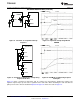
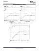
The start and stop voltages for typical 3.3-V and 5-V output applications are shown in Figure 25 and Figure 26.
The voltages are plotted versus load current. The start voltage is defined as the input voltage needed to regulate
the output within 1%. The stop voltage is defined as the input voltage at which the output drops by 5% or stops
switching.
During high duty cycle conditions, the inductor current ripple increases while the BOOT capacitor is being
recharged resulting in an increase in ripple voltage on the output. This is due to the recharge time of the boot
capacitor being longer than the typical high-side off time when switching occurs every cycle.
Figure 25. 3.3-V Start/Stop Voltage Figure 26. 5-V Start/Stop Voltage
Error Amplifier
The TPS54260-Q1 has a transconductance amplifier for the error amplifier. The error amplifier compares the
VSENSE voltage to the lower of the SS/TR pin voltage or the internal 0.8-V voltage reference. The
transconductance (gm) of the error amplifier is 310 μA/V during normal operation. During the slow start
operation, the transconductance is a fraction of the normal operating gm. When the voltage of the VSENSE pin is
below 0.8 V and the device is regulating using the SS/TR voltage, the gm is 70 μA/V.
The frequency compensation components (capacitor, series resistor and capacitor) are added to the COMP pin
to ground.
Voltage Reference
The voltage reference system produces a precise ±2% voltage reference over temperature by scaling the output
of a temperature stable bandgap circuit.
Adjusting the Output Voltage
The output voltage is set with a resistor divider from the output node to the VSENSE pin. TI recommends to use
1% tolerance or better divider resistors. Start with a 10 kΩ for the R2 resistor and use the Equation 1 to calculate
R1. To improve efficiency at light loads consider using larger value resistors. If the values are too high the
regulator is more susceptible to noise and voltage errors from the VSENSE input current is noticeable.
14 Submit Documentation Feedback Copyright © 2010–2013, Texas Instruments Incorporated
Product Folder Links: TPS54260-Q1