
Datasheet


BOOT
VIN
EN
SS/TR
RT/CLK
PH
GND
COMP
VSENSE
PWRGD
Input
Bypass
Capacitor
UVLO
Adjust
Resistors
SlowStart
Capacitor
Frequency
SetResistor
Compensation
Network
Resistor
Divider
Output
Inductor
Output
Capacitor
Vout
Vin
Topside
Ground
Area
Catch
Diode
RouteBootCapacitor
Traceonanotherlayerto
providewidepathfor
topsideground
ThermalVIA
SignalVIA
TPS54240-Q1
SLVSAQ4B –DECEMBER 2010 –REVISED SEPTEMBER 2013
www.ti.com
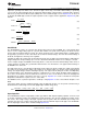
Layout
Layout is a critical portion of good power supply design. There are several signals paths that conduct fast
changing currents or voltages that can interact with stray inductance or parasitic capacitance to generate noise
or degrade the power supplies performance. To help eliminate these problems, the VIN pin should be bypassed
to ground with a low ESR ceramic bypass capacitor with X5R or X7R dielectric. Care should be taken to
minimize the loop area formed by the bypass capacitor connections, the VIN pin, and the anode of the catch
diode. See Figure 63 for a PCB layout example. The GND pin should be tied directly to the power pad under the
IC and the power pad.
The power pad should be connected to any internal PCB ground planes using multiple vias directly under the IC.
The PH pin should be routed to the cathode of the catch diode and to the output inductor. Because the PH
connection is the switching node, the catch diode and output inductor should be located close to the PH pins,
and the area of the PCB conductor minimized to prevent excessive capacitive coupling. For operation at full rated
load, the top side ground area must provide adequate heat dissipating area. The RT/CLK pin is sensitive to noise
so the RT resistor should be located as close as possible to the IC and routed with minimal lengths of trace. The
additional external components can be placed approximately as shown. It may be possible to obtain acceptable
performance with alternate PCB layouts, however this layout has been shown to produce good results and is
meant as a guideline.
Figure 63. PCB Layout Example
38 Submit Documentation Feedback Copyright © 2010–2013, Texas Instruments Incorporated
Product Folder Links: TPS54240-Q1