
Datasheet


TPS54240-Q1
SLVSAQ4B –DECEMBER 2010 –REVISED SEPTEMBER 2013
www.ti.com
DETAILED DESCRIPTION (continued)
The PWRGD pin is pulled low when the VSENSE is lower than 92% or greater than 109% of the nominal internal
reference voltage. Also, the PWRGD is pulled low, if the UVLO or thermal shutdown are asserted or the EN pin
pulled low.
Overvoltage Transient Protection
The TPS54240-Q1 incorporates an overvoltage transient protection (OVTP) circuit to minimize voltage overshoot
when recovering from output fault conditions or strong unload transients on power supply designs with low value
output capacitance. For example, when the power supply output is overloaded the error amplifier compares the
actual output voltage to the internal reference voltage. If the VSENSE pin voltage is lower than the internal
reference voltage for a considerable time, the output of the error amplifier responds by clamping the error
amplifier output to a high voltage. Thus, requesting the maximum output current. Once the condition is removed,
the regulator output rises and the error amplifier output transitions to the steady state duty cycle. In some
applications, the power supply output voltage can respond faster than the error amplifier output can respond, this
actuality leads to the possibility of an output overshoot. The OVTP feature minimizes the output overshoot, when
using a low value output capacitor, by implementing a circuit to compare the VSENSE pin voltage to OVTP
threshold which is 109% of the internal voltage reference. If the VSENSE pin voltage is greater than the OVTP
threshold, the high side MOSFET is disabled preventing current from flowing to the output and minimizing output
overshoot. When the VSENSE voltage drops lower than the OVTP threshold, the high side MOSFET is allowed
to turn on at the next clock cycle.
Thermal Shutdown
The device implements an internal thermal shutdown to protect itself if the junction temperature exceeds 182°C.
The thermal shutdown forces the device to stop switching when the junction temperature exceeds the thermal
trip threshold. Once the die temperature decreases below 182°C, the device reinitiates the power up sequence
by discharging the SS/TR pin.
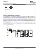
Small Signal Model for Loop Response
Figure 46 shows an equivalent model for the TPS54240-Q1 control loop which can be modeled in a circuit
simulation program to check frequency response and dynamic load response. The error amplifier is a
transconductance amplifier with a g
mEA
of 310 μA/V. The error amplifier can be modeled using an ideal voltage
controlled current source. The resistor R
o
and capacitor C
o
model the open loop gain and frequency response of
the amplifier. The 1-mV ac voltage source between the nodes a and b effectively breaks the control loop for the
frequency response measurements. Plotting c/a shows the small signal response of the frequency compensation.
Plotting a/b shows the small signal response of the overall loop. The dynamic loop response can be checked by
replacing R
L
with a current source with the appropriate load step amplitude and step rate in a time domain
analysis. This equivalent model is only valid for continuous conduction mode designs.
24 Submit Documentation Feedback Copyright © 2010–2013, Texas Instruments Incorporated
Product Folder Links: TPS54240-Q1