
Datasheet


TPS51604
SLUSBA6A –DECEMBER 2012–REVISED AUGUST 2013
www.ti.com
These devices have limited built-in ESD protection. The leads should be shorted together or the device placed in conductive foam
during storage or handling to prevent electrostatic damage to the MOS gates.
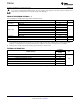
ABSOLUTE MAXIMUM RATINGS
(1) (2)
over operating free-air temperature range (unless otherwise noted)
MIN MAX UNIT
VDD –0.3 6
Input voltage V
PWM, SKIP –0.3 6
BST –0.3 35
BST (transient < 20 ns) –0.3 38
BST to SW; DRVH to SW –0.3 6
Output voltage V
SW –2 30
DRVH, SW (transient < 20 ns) –5 38
DRVL –0.3 6
Ground pins GND to PAD –0.3 0.3 V
Operating junction temperature, T
J
–40 125 °C
Storage temperature, T
stg
–55 150 °C
(1) Stresses beyond those listed under "absolute maximum ratings" may cause permanent damage to the device. These are stress ratings
only and functional operation of the device at these or any other conditions beyond those indicated under "recommended operating
conditions" is not implied. Exposure to absolute-maximum-rated conditions for extended periods may affect device reliability.
(2) All voltage values are with respect to the network ground terminal unless otherwise noted.
THERMAL INFORMATION
TPS51604
THERMAL METRIC
(1)
UNIT
WSON (DSG)
(8 PINS)
θ
JA
Junction-to-ambient thermal resistance 63.1
θ
JCtop
Junction-to-case (top) thermal resistance 74.1
θ
JB
Junction-to-board thermal resistance 34.3
°C/W
ψ
JT
Junction-to-top characterization parameter 2.0
ψ
JB
Junction-to-board characterization parameter 34.9
θ
JCbot
Junction-to-case (bottom) thermal resistance 11.7
(1) For more information about traditional and new thermal metrics, see the IC Package Thermal Metrics application report, SPRA953.
2 Submit Documentation Feedback Copyright © 2012–2013, Texas Instruments Incorporated
Product Folder Links: TPS51604