
Datasheet


www.ti.com
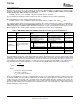
LAYOUT CONSIDERATIONS
TPS51200
SLUS812 – FEBRUARY 2008
For further information regarding the PowerPAD™ package and the recommended board layout, refer to the
PowerPAD™ package application note (SLMA002 ). This document is available at www.ti.com .
Consider the following points before starting the TPS51200 layout design.
• The input bypass capacitor for VLDOIN should be placed as close as possible to the pin with short and wide
connections.
• The output capacitor for VO should be placed close to the pin with short and wide connection in order to
avoid additional ESR and/or ESL trace inductance.
• VOSNS should be connected to the positive node of VO output capacitor(s) as a separate trace from the high
current power line. This configuration is strongly recommended to avoid additional ESR and/or ESL. If
sensing the voltage at the point of the load is required, it is recommended to attach the output capacitor(s) at
that point. Also, it is recommended to minimize any additional ESR and/or ESL of ground trace between the
GND pin and the output capacitor(s).
• Consider adding low-pass filter at VOSNS if the ESR of the VO output capacitor(s) is larger than 2 m Ω .
• REFIN can be connected separately from VLDOIN. Remember that this sensing potential is the reference
voltage of REFOUT. Avoid any noise-generating lines.
• The negative node of the VO output capacitor(s) and the REFOUT capacitor should be tied together by
avoiding common impedance to the high current path of the VO source/sink current.
• The GND and PGND pins should be connected to the thermal land underneath the die pad with multiple vias
connecting to the internal system ground planes (for better result, use at least two internal ground planes).
Use as many vias as possible to reduce the impedance between PGND/GND and the system ground plane.
Also, place bulk caps close to the DIMM load point, route the VOSNS to the DIMM load sense point.
• In order to effectively remove heat from the package, properly prepare the thermal land. Apply solder directly
to the package ’ s thermal pad. The wide traces of the component and the side copper connected to the
thermal land pad help to dissipate heat. Numerous vias 0,33 mm in diameter connected from the thermal land
to the internal/solder side ground plane(s) should also be used to help dissipation.
• Please consult the TPS51200-EVM User's Guide (SLUUxxx) for detailed layout recommendations.
Copyright © 2008, Texas Instruments Incorporated 17
Product Folder Link(s): TPS51200