
Datasheet


www.ti.com
TPS51200
SLUS812 – FEBRUARY 2008
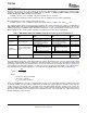
Figure 5. Bode Plot for a Typical DDR3 Configuration
Figure 5 shows the bode plot simulation for a typical DDR3 configuration of the TPS51200, where:
• V
IN
= 3.3 V
• V
VLDOIN
= 1.5 V
• V
VO
= 0.75 V
• I
IO
= 2 A
• 3 × 10- µ F capacitors included
• ESR = 2.5 m Ω
• ESL = 800 pH
The unity-gain bandwidth is approximately 1 MHz and the phase margin is 52 ° . The 0-dB level is crossed, the
gain peaks because of the ESL effect. However, the peaking is kept well below 0 dB.
Figure 6 shows the load regulation and Figure 7 shows the transient response for a typical DDR3 configuration.
When the regulator is subjected to ± 1.5-A load step and release, the output voltage measurement shows no
difference between the dc and ac conditions.
Copyright © 2008, Texas Instruments Incorporated 13
Product Folder Link(s): TPS51200