
Datasheet


TPS5103
MULTIPLE MODE SYNCHRONOUS DC/DC CONTROLLER
SLVS240A – SEPTEMBER 1999 – REVISED MAY 2001
24
POST OFFICE BOX 655303 • DALLAS, TEXAS 75265
APPLICATION INFORMATION
loop-gain compensation
Voltage mode control is used in this controller for the output voltage regulation. To achieve fast, stabilized
control, two parts are discussed in this section: the power stage small signal modeling and the compensation
circuit design.
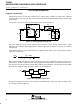
For the buck converter, the small-signal modeling circuit is shown in Figure 41.
+
–
ac
i
a
i
c
p
D
1
V
ap
D
d
∧
I
c
d
∧
+
V
I
R
L
L
Z
L
C
R
R
C
Z
RC
V
O
Figure 41. Small-Signal Modeling Circuit
From this equivalent circuit, several control transfer functions can be derived: input-to-output, output
impedance, and control-to-output. Typically, the control-to-output transfer function is used for the feedback
control design.
Assuming R
C
and R
L
are much smaller than R, the simplified small signal control-to-output transfer function
equation is shown below.
Vod
d
(
1 sCRc
)
1 s
C Rc R
L
L
R
s
2
LC
∧
∧
Where C is the output capacitance, Rc is the equivalent serial resistance (ESR) in the output capacitor, L is the
output inductor, RL is the equivalent serial resistance (ESR) in the output inductor, and R is the load resistance.
To achieve the fast transient response and the better output voltage regulation, a compensation circuit is added
to improve the feedback control. The whole system is shown in Figure 42.
PWM
Power
Stage
Compensation
V
ref
Figure 42. Loop-Gain Compensation
The typical compensation circuit used as an option in the EVM design is a part of the output feedback circuit.
The circuitry is shown in Figure 43.