
Datasheet


1
2
3
4
5
6
7
8
9
10
11
12
13
14
15
16
17
18
19
20
21
22
23
24
25
26
27
28
29
30
31
32
33
34
35
36
37
38
VBAT
DS
GC1
GC2
CBA
GA1
PHA
GA2
PGNDA
SA1
SA2
FBA
COMPA
SSA
PGA
ENA
ENB
COMPC
ENC SYNC
DLYAB
RT
AGND
PGB
SSB
COMPB
FBB
SB2
SB1
PGNDB
GB2
PHB
GB1
CBB
VREG
DIV
EXTSUP
VIN
TPS43330-Q1
TPS43332-Q1
www.ti.com
SLVSA82E –MARCH 2011–REVISED APRIL 2013
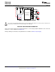
DEVICE INFORMATION
DAP PACKAGE
(TOP VIEW)
PIN FUNCTIONS
NAME NO. I/O DESCRIPTION
AGND 23 O Analog ground reference
A capacitor on this pin acts as the voltage supply for the high-side N-channel MOSFET gate-drive circuitry in buck
CBA 5 I controller BuckA. When the buck is in a dropout condition, the device automatically reduces the duty cycle of the
high-side MOSFET to approximately 95% on every fourth cycle to allow the capacitor to recharge.
A capacitor on this pin acts as the voltage supply for the high-side N-channel MOSFET gate-drive circuitry in buck
CBB 34 I controller BuckB. When the buck is in a dropout condition, the device automatically reduces the duty cycle of the
high-side MOSFET to approximately 95% on every fourth cycle to allow the capacitor to recharge.
Error amplifier output of BuckA and compensation node for voltage-loop stability. The voltage at this node sets the
COMPA 13 O target for the peak current through the inductor of BuckA. Clamping this voltage on the upper and lower ends
provides current-limit protection for the external MOSFETs.
Error amplifier output of BuckB and compensation node for voltage-loop stability. The voltage at this node sets the
COMPB 26 O target for the peak current through the inductor of BuckB. Clamping this voltage on the upper and lower ends
provides current-limit protection for the external MOSFETs.
COMPC 18 O Error-amplifier output and loop-compensation node of the boost regulator
The status of this pin defines the output voltage of the boost regulator. A high input regulates the boost converter
DIV 36 I at 11 V, a low input sets the value at 7 V, and a floating pin sets 10 V. NOTE: DIV = high and ENC = high inhibits
low-power mode on the bucks.
The capacitor at the DLYAB pin sets the power-good delay interval used to de-glitch the outputs of the power-
DLYAB 21 O
good comparators. Leaving this pin open sets the power-good delay to an internal default value of 20 µs typical.
This input monitors the voltage on the external boost-converter low-side MOSFET for overcurrent protection. An
DS 2 I alternative connection for better noise immunity is to a sense resistor between the source of the low-side
MOSFET and ground via a filter network.
Enable input for BuckA (active-high with an internal pullup current source). An input voltage higher than 1.7 V
ENA 16 I enables the controller, whereas an input voltage lower than 0.7 V disables the controller. When both ENA and
ENB are low, the device shuts down and consumes less than 4 µA of current.
Copyright © 2011–2013, Texas Instruments Incorporated Submit Documentation Feedback 9
Product Folder Links: TPS43330-Q1 TPS43332-Q1