
Datasheet


RIPPLE
PK OUT
I
2.10
I I 10 11.05 A
2 2
= + = + =
( )
( )
( )
( )
2 2
2
2
RIPPLE
LOUT _RMS OUT
I 2.10
I I 10 10.02 A
12 12
= + = + =
f
IN(max) OUT
OUT
RIPPLE
IN(max) SW OUT
(V V )
V
1.83 V (13.2 V 1.83 V)
I 2.10 A
V L 13.2 V 300kHz 2.5 H
-
-
= ´ = ´ =
´ ´ m
f
IN(max) OUT
OUT
OUT
IN(max) SW RIPPLE
(V - V )
V
1.8 V (13.2 V - 1.8 V)
L 2.59 H
V I 13.2 V 300kHz 2.0
= ´ = ´ = m
´ ´
TPS40195
SLUS720E –FEBRUARY 2007–REVISED JULY 2012
www.ti.com
Schematic
This section discusses basic buck converter design. Designers already familiar with the design of buck
converters can skip to the next section Component Selection of this design example.
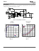
Figure 24. TPS40195 Design Example Schematic
Output Inductor, L
OUT
Equation 9 can be used to calculate L
OUT
.
where
• I
RIPPLE
= the allowable ripple current in the inductor, 20% of maximum I
OUT
(9)
For this design a 2.5-μH inductor from Coilcraft is used. I
RIPPLE
is recalculated using Equation 10 and a 2.5-μH
inductor value to give a new estimate of I
RIPPLE
of 2.1 A .
(10)
With this I
RIPPLE
value, the RMS and peak current flowing in L
OUT
can be calculated.
(11)
(12)
22 Copyright © 2007–2012, Texas Instruments Incorporated