
Datasheet


( )
( )
J A
Q
JA IN
SW
T T
I
V
f Hz
2 Qg
æ ö
æ ö
-
ç ÷
-
ç ÷
ç ÷
q ´
ç ÷
è ø
=
ç ÷
´
ç ÷
ç ÷
è ø
TPS40054
TPS40055
TPS40057
www.ti.com
SLUS593H –DECEMBER 2003–REVISED JULY 2012
(46)
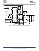
LAYOUT CONSIDERATIONS
MOSFET PACKAGING
MOSFET package selection depends on MOSFET power dissipation and the projected operating conditions. In
general, for a surface-mount applications, the DPAK style package provides the lowest thermal impedance (θ
JA
)
and, therefore, the highest power dissipation capability. However, the effectiveness of the DPAK depends on
proper layout and thermal management. The θ
JA
specified in the MOSFET data sheet refers to a given copper
area and thickness. In most cases, a lowest thermal impedance of 40°C/W requires one square inch of 2-ounce
copper on a G-10/FR-4 board. Lower thermal impedances can be achieved at the expense of board area. Please
refer to the selected MOSFET's data sheet for more information regarding proper mounting.
GROUNDING AND CIRCUIT LAYOUT CONSIDERATIONS
The TPS4005x provides separate signal ground (SGND) and power ground (PGND) pins. It is important that
circuit grounds are properly separated. Each ground should consist of a plane to minimize its impedance if
possible. The high power noisy circuits such as the output, synchronous rectifier, MOSFET driver decoupling
capacitor (BP10), and the input capacitor should be connected to PGND plane at the input capacitor.
Sensitive nodes such as the FB resistor divider, R
T
, and ILIM should be connected to the SGND plane. The
SGND plane should only make a single point connection to the PGND plane.
Component placement should ensure that bypass capacitors (BP10 and BP5) are located as close as possible to
their respective power and ground pins. Also, sensitive circuits such as FB, RT and ILIM should not be located
near high dv/dt nodes such as HDRV, LDRV, BOOST, and the switch node (SW).
Copyright © 2003–2012, Texas Instruments Incorporated Submit Documentation Feedback 21
Product Folder Link(s): TPS40054 TPS40055 TPS40057