
Datasheet


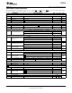


Table Of Contents
- FEATURES
- APPLICATIONS
- DESCRIPTION
- ABSOLUTE MAXIMUM RATINGS
- DISSIPATION RATINGS
- RECOMMENDED OPERATING CONDITIONS
- ELECTRICAL CHARACTERISTICS
- DEVICE INFORMATION
- TYPICAL CHARACTERISTICS through .
- APPLICATION INFORMATION
- REVISION HISTORY

2
IN IN MIN LIM _ MIN
MIN OUT
V V 4 R P
R I V
2
± - ´ ´
´ = =
2
IN IN MIN LIM _ MIN
MIN
V V 4 R P
I
2 R
± - ´ ´
=
´
2
MIN IN LIM _ MIN
R I V I P 0´ - ´ + =
2
LOAD LIM LOAD IN
ON
2
LIM
LIM
C ×P C ×V
t = +
2×P
2×I
TPS2590
SLUS960F –JULY 2009–REVISED MAY 2013
www.ti.com
APPLICATION INFORMATION
Startup
Large inrush current occurs when power is applied to discharged capacitors and load. During the inrush period,
the TPS2590 operates in power limit (or SOA protect mode) managing the current as VOUT rises. In SOA
protect mode, the internal MOSFET power dissipation ([V
IN
– V
OUT
] x I
OUT
) is regulated at 5W typical while the
fault timer starts and C
CT
ramps up. As the charge builds on C
LOAD
, the current increases towards I
LIM
. When the
capacitor is fully charged, I
OUT
drops to the dc load value, the fault timer stops, and C
CT
ramps down. In order for
the TPS2590 to start properly, the fault timer duration must exceed C
LOAD
start up time, t
ON
. Start up time without
additional dc loading can be determined using Equation 6 where P
LIM
= 5W (typical).
(6)
When the load has a resistive component in addition to C
LOAD
, the fault time must be extended because the
resistive load current is unavailable to charge C
LOAD
. Table 1 and Table 2 can be used to predict start up time in
the presence of resistive dc loading.
Refer to the TPS2590 Design Calculator Tool (SLUC398) for assistance with design calculations.
Table 1. Start up Time (ms) with DC Loading: V
IN
=5V, P
LIM
=3W, I
LIM
=5A
R
LOAD_
(Ω) C
LOAD_
= 100 µF C
LOAD_
= 220 µF C
LOAD_
= 470 µF C
LOAD_
= 1000 µF
1000 0.43 0.95 2.03 4.33
10 0.5 1.11 2.36 5.03
5 0.61 1.34 2.87 6.1
3 0.91 2 4.28 9.11
2.5 1.31 2.88 6.14 13.07
Table 2. Start up Time (ms) with DC Loading: V
IN
=12V, P
LIM
=3W, I
LIM
=5A
R
LOAD_
(Ω) C
LOAD_
= 100 µF C
LOAD_
= 220 µF C
LOAD_
= 470 µF C
LOAD_
= 1000 µF
10000 2.46 5.41 11.56 24.59
100 2.67 5.87 12.55 26.69
50 2.93 6.45 13.79 29.34
15 6.7 14.74 31.5 67.01
13 11.68 25.69 54.87 116.75
Maximum Allowable Load to Ensure Successful Start up
The power limiting function of the TPS2590 provides very effective protection for the internal FET. Expectedly,
there is a supply voltage dependent maximum allowable load required for successful startup. Loads above this
can cause the output to shut off due to CT timeout or thermal shutdown because V
OUT
hangs at an intermediate
voltage below V
IN
. The equation for maximum load (or R
MIN
is derived using the circuit equations for V
OUT
as a
function of V
IN
, R
LOAD
, P
LIM
, and the result is quadratic in form.
(7)
(8)
(9)
When R
LOAD
< R
MIN
, the numerical result for V
OUT
is real (V
IN
2
– 4 × R
LOAD
× P
LIM
> 0) and less than V
IN
meaning
the circuit will not start (CT or thermal shutdown). When R
LOAD
> R
MIN
, the numerical result for V
OUT
is imaginary
(V
IN
2
– 4 × R
LOAD
x P
LIM
< 0) and the circuit will start (V
OUT
= V
IN
). Ensure that R
LOAD
is > R
MIN
per Equation 11.
10 Submit Documentation Feedback Copyright © 2009–2013, Texas Instruments Incorporated
Product Folder Links: TPS2590