
Datasheet


TPS24720
SLVSAL1C –MARCH 2011–REVISED SEPTEMBER 2013
www.ti.com
GATE: This pin provides gate drive to the external MOSFET. A charge pump sources 30 µA to enhance the
external MOSFET. A 13.9-V clamp between GATE and VCC limits the gate-to-source voltage, because V
VCC
is
very close to V
OUT
in normal operation. During start-up, a transconductance amplifier regulates the gate voltage
of M
1
to provide inrush current limiting. The TIMER pin charges timer capacitor C
T
during the inrush. Inrush
current limiting continues until the V
(GATE – VCC)
exceeds the Timer Activation Voltage (5.9 V for V
VCC
= 12 V).
Then the TPS24720 enters into circuit-breaker mode. The Timer Activation Voltage is defined as a threshold
voltage. When V
(GATE-VCC)
exceeds this threshold voltage, the inrush operation is finished and the TIMER stops
sourcing current and begins sinking current. In the circuit-breaker mode, the current flowing in R
SENSE
is
compared with the current-limit threshold derived from the MOSFET power-limit scheme (see PROG). If the
current flowing in R
SENSE
exceeds the current limit threshold, then MOSFET M
1
is turned off. The GATE pin is
disabled by the following three mechanisms:
1. GATE is pulled down by an 11-mA current source when
– The fault timer expires during an overload current fault (V
IMON
> 675 mV)
– V
EN
is below its falling threshold
– V
VCC
drops below the UVLO threshold
– V
OV
is above its rising threshold
2. GATE is pulled down by a 1-A current source for 13.5 µs when a hard output short circuit occurs and V
(VCC –
SENSE)
is greater than 60 mV, i.e., the fast-trip shutdown threshold. After fast-trip shutdown is complete, an
11-mA sustaining current ensures that the external MOSFET remains off.
3. GATE is discharged by a 20-kΩ resistor to GND if the chip die temperature exceeds the OTSD rising
threshold or ENSD is pulled low.
GATE remains low in latch mode and attempts a restart periodically in retry mode.
If used, any capacitor connecting GATE and GND should not exceed 1 μF and it should be connected in series
with a resistor of no less than 1 kΩ. No external resistor should be directly connected from GATE to GND or from
GATE to OUT.
GND: This pin is connected to system ground.
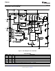
IMON: A resistor connected from this pin to GND scales the current-limit and power-limit settings, as illustrated in
Figure 5. The voltage present at this pin is proportional to the current flowing through sense resistor R
SENSE
. This
voltage can be used as a means of monitoring current flow through the system. The value of R
IMON
can be
calculated from Equation 3. This pin should not have a bypass capacitor or any other load except for R
IMON
.
LATCH: This pin determines whether the TPS24720 operates in latch mode or retry mode. Applying a voltage of
2 V to 5 V to this pin or allowing it to float selects latch mode. Tying the pin to ground selects retry mode. In latch
mode, an overload current fault disables the TPS24720 until EN, ENSD, or VCC is cycled. In retry mode, the
TPS24720 automatically attempts a restart after every sixteen cycles of TIMER charging and discharging. In a
sustained fault in retry mode, the external MOSFET conducts 3.93% of the time; i.e., the duty ratio is 0.0393. If
the LATCH pin is allowed to float, then its open-circuit voltage is approximately 2.28 V.
OUT: This pin allows the controller to measure the drain-to-source voltage across the external MOSFET M
1
. The
power-good indicator (PGb) relies on this information, as does the power-limiting engine. The OUT pin should be
protected from negative voltage transients by a clamping diode or sufficient capacitors. A Schottky diode of 3 A /
40 V in a SMC package is recommended as a clamping diode for high-power applications. The OUT pin should
be bypassed to GND with a low-impedance ceramic capacitor in the range of 10 nF to 1 µF.
OV: This pin is used to program the device overvoltage level. A voltage of more than 1.35 V on this pin turns off
the external MOSFET. A resistor divider connected from VCC to this pin provides overvoltage protection for the
downstream load. This pin should be tied to GND when not used.
PGb: This active-low, open-drain output is intended to interface to downstream dc/dc converters or monitoring
circuits. PGb pulls low after the drain-to-source voltage of the FET has fallen below 170 mV and a 3.4-ms
deglitch delay has elapsed. It goes open-drain when V
DS
exceeds 240 mV. PGb assumes high-impedance status
after a 3.4-ms deglitch delay once V
DS
of M
1
rises up, resulting from GATE being pulled to GND at any of the
following conditions :
• An overload current fault occurs (V
IMON
> 675 mV).
• A hard output short circuit occurs, leading to V
(VCC – SENSE)
greater than 60 mV, i.e., the fast-trip shutdown
threshold has been exceeded.
• V
EN
is below its falling threshold.
8 Submit Documentation Feedback Copyright © 2011–2013, Texas Instruments Incorporated
Product Folder Links: TPS24720