
Datasheet


TPS24720
www.ti.com
SLVSAL1C –MARCH 2011–REVISED SEPTEMBER 2013
PIN FUNCTIONS (continued)
NAME PIN I/O DESCRIPTION
Latch or retry mode select input. Latch when floating or connected to a logic-level voltage; retry when
LATCH 14 I
connected to GND.
OUT 8 I Output voltage sensor for monitoring MOSFET power.
Overvoltage comparator input. Connects to resistor divider. GATE is pulled low when OV exceeds the
OV 5 I
threshold.
PGb 15 O Active-low, open-drain power-good indicator. Status is determined by the voltage across the MOSFET.
Power-limiting programming pin. A resistor from this pin to GND sets the maximum power dissipation for the
PROG 2 I
FET.
SENSE 11 I Current-sensing input for resistor shunt from VCC to SENSE.
SET 7 I Current-limit programming set pin. A resistor is connected from this pin to VCC.
TIMER 3 I/O A capacitor connected from this pin to GND provides a fault timing function.
VCC 12 I Input-voltage sense and power supply
Thermal
— — Tied to GND
pad
DETAILED PIN DESCRIPTIONS
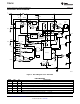
The following description relies on the typical application diagram shown on the front page of this data sheet, as
well as the functional block diagram in Figure 5.
EN: Applying a voltage of 1.35 V or more to this pin enables the gate driver. The addition of an external resistor
divider allows the EN pin to serve as an undervoltage monitor. Cycling EN low and then back high resets the
TPS24720 that has latched off due to a fault condition. This pin should not be left floating.
ENSD: When this pin is pulled low, it shuts off all internal circuitry and thus places the device in a low-current
standby mode. While in standby, the PGb, FLTb, and FFLTb outputs assume high-impedance states. A 20-kΩ
resistor pulls GATE to GND in standby. This is a much weaker pulldown than the 11 mA drawn while the part is
disabled (e.g., by EN, UVLO, OV, or overload fault current). Applications requiring rapid turnoff should disable
the device using the EN pin before pulling ENSD low. This pin is preferably pulled up to a positive voltage from
2 V to 18 V, if not otherwise connected.
FFLTb: This active-low open-drain output pulls low if V
VCC
is higher than the UVLO rising threshold and the
voltage on the IMON pin exceeds 103 mV when EN is disabled. The presence of this voltage indicates that
current continues to flow through the external circuitry even though the external MOSFET has been turned off.
This presumably indicates a shorted MOSFET. FFLTb assumes a high impedance if one of the following
conditions occurs:
• ENSD is pulled low.
• Temperature on the die exceeds the OTSD shutdown threshold.
• V
VCC
drops below the UVLO falling threshold.
FFLTb also asserts if V
VCC
is higher than the UVLO rising threshold, GATE is disabled by OV, and the voltage on
the IMON pin exceeds 103 mV. This pin can be left floating when not used.
FLTb: This active-low open-drain output pulls low when the TPS24720 has remained in current limit long enough
for the fault timer to expire. The behavior of the FLTb pin depends on the status of the LATCH pin. If the LATCH
pin is held high or left floating, the TPS24720 operates in latch mode. If the LATCH pin is held low, the
TPS24720 operates in retry mode. In latch mode, a fault timeout disables the external MOSFET and holds FLTb
low. The latched mode of operation is reset by cycling EN, VCC, or ENSD. In retry mode, a fault timeout first
disables the external MOSFET, next waits sixteen cycles of TIMER charging and discharging, and finally
attempts a restart. This process repeats as long as the fault persists. In retry mode, the FLTb pin is pulled low
whenever the external MOSFET is disabled by the fault timer. In a sustained fault, the FLTb waveform becomes
a train of pulses. The FLTb pin does not assert if the external MOSFET is disabled by EN, ENSD, OV,
overtemperature shutdown, or UVLO. This pin can be left floating when not used.
Copyright © 2011–2013, Texas Instruments Incorporated Submit Documentation Feedback 7
Product Folder Links: TPS24720