
Datasheet


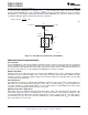


OUT VCC
CHG
C V
t
I
´
D =
2
ENTHRESH VCC
1 2
R
V V
R R
= ´
+
G009
1k
10
0.01
1
100
I – Drain-to-Source Current – A
DS
0.1
0.01 0.1 10 1001
Single Pulse
R = 94ºC/W (min Cu)
θJA
1ms
10ms
100ms
1s
DC
Area Limited
by R
DS(on)
V – Drain-to-Source Voltage – V
DS
TPS24710, TPS24711
TPS24712, TPS24713
www.ti.com
SLVSAL2E –JANUARY 2011–REVISED NOVEMBER 2013
Figure 35. CSD16403Q5 SOA Curve
STEP 5. Calculate the Retry-Mode Duty Ratio
In retry mode, the TPS24711/13 is on for one charging cycle and off for 16 charge/discharge cycles, as can be
seen in Figure 32. The first C
T
charging cycle is from 0 V to 1.35 V, which gives 7.56 ms. The first C
T
discharging
cycle is from 1.35 V to 0.35 V, which gives 5.6 ms. Therefore, the total time is 7.56 ms + 33 × 5.6 ms = 192.36
ms. As a result, the retry mode duty ratio is 7.56 ms/192.36 ms = 3.93%.
STEP 6. Select R
1
and R
2
for UV
Next, select the values of the UV resistors, R
1
and R
2
, as shown in the typical application diagram on the front
page. From the TPS24710/11/12/13 electrical specifications, V
ENTHRESH
= 1.35 V. The V
UV
is the undervoltage
trip voltage, which for this example equals 10.7 V.
(13)
Assume R
1
is 130 kΩ and use Equation 13 to solve for the R
2
value of 18.7 kΩ.
STEP 7. Choose R
GATE
, R
4
, R
5
and C
1
In the typical application diagram on the front page, the gate resistor, R
GATE
, is intended to suppress high-
frequency oscillations. A resistor of 10 Ω will serve for most applications, but if M
1
has a C
ISS
below 200 pF, then
33 Ω is recommended. Applications with larger MOSFETs and very short wiring may not require R
GATE
. R
4
and
R
5
are required only if PGb and FLTb are used; these resistors serve as pullups for the open-drain output
drivers. The current sunk by each of these pins should not exceed 2 mA (see the RECOMMENDED
OPERATING CONDITIONS table). C
1
is a bypass capacitor to help control transient voltages, unit emissions,
and local supply noise while in the disabled state. Where acceptable, a value in the range of 0.001 μF to 0.1 μF
is recommended.
ALTERNATIVE DESIGN EXAMPLE: GATE CAPACITOR (dV/dt) CONTROL IN INRUSH MODE
The TPS24710/11/12/13 can be used in applications that expect a constant inrush current. This current is
controlled by a capacitor connected from the GATE terminal to GND. A resistor of 1 kΩ placed in series with this
capacitor will prevent it from slowing a fast-turnoff event. In this mode of operation, M
1
operates as a source
follower, and the slew rate of the output voltage approximately equals the slew rate of the gate voltage (see
Figure 36).
To implement a constant-inrush-current circuit, choose the time to charge, ∆t, using Equation 14,
(14)
where C
OUT
is the output capacitance, V
VCC
is the input voltage, and I
CHG
is the desired charge current. Choose
I
CHG
< P
LIM
/ V
VCC
to prevent power limiting from affecting the desired current.
Copyright © 2011–2013, Texas Instruments Incorporated Submit Documentation Feedback 25
Product Folder Links: TPS24710 TPS24711 TPS24712 TPS24713