
Datasheet


LOADPROTECTION
0.1 Fμ 0.1 Fμ
B0440-03
M
1
12-VMainBusSupply
TIMER
OUT
GATE
VCC
SENSE
GND
TPS2470x
Specifications(atOutput):
PeakCurrentLimit=12 A
NominalCurrent=10 A
R
1.2
LOAD
W
C
470 F
OUT
μ
C
T
R
SENSE
R
GATE
( )
VCC SENSE
SENSE
LIM
SENSE
V
R ,
I
therefore,
25 mV
R 2 m
12 A
-
=
= » W
TPS24700
TPS24701
SLVSAL3B – MARCH 2011– REVISED MAY 2011
www.ti.com
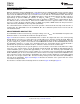
DESIGN EXAMPLE: CURRENT-LIMITED START-UP
This design example assumes a 12-V system voltage with an operating tolerance of ±2 V. The rated load current
is 10 A, corresponding to a dc load of 1.2 Ω. If the current exceeds 12 A, then the controller should shut down
and then attempt to restart. Ambient temperatures may range from 20°C to 50°C. The load has a minimum input
capacitance of 470 μF. Figure 30 shows a simplified system block diagram of the proposed application.
This design procedure seeks to control the junction temperature of MOSFET M1 under both static and transient
conditions by proper selection of package, cooling, r
DS(on)
, current limit, fault timeout, and power limit. The design
procedure further assumes that a unit running at full load and maximum ambient temperature experiences a brief
input power interruption sufficient to discharge C
OUT
, but short enough to keep M1 from cooling. A full C
OUT
recharge then takes place. Adjust this procedure to fit your application and design criteria.
Figure 30. Simplified Block Diagram of the System Constructed in the Design Example
STEP 1. Choose R
SENSE
From the TPS24700/1 electrical specifications, the typical current-limit threshold voltage, V
(VCC–SENSE)
, is 25 mV.
A resistance of 2 mΩ is selected for the peak current limit of 12 A, while dissipating only 200 mW at the rated
10-A current (see Equation 3). This represents a 0.17% power loss.
(3)
STEP 2. Choose MOSFET M1
The next design step is to select M1. The TPS24700/1 is designed to use an N-channel MOSFET with a
gate-to-source voltage rating of 20 V.
Devices with lower gate-to-source voltage ratings can be used if a Zener diode is connected to limit the
maximum gate-to-source voltage across the transistor.
The next factor to consider is the drain-to-source voltage rating, V
DS(MAX)
, of the MOSFET. Although the
MOSFET only sees 12 V dc, it may experience much higher transient voltages during extreme conditions, such
as the abrupt shutoff that occurs during a fast trip. A TVS may be required to limit inductive transients under such
conditions. A transistor with a V
DS(MAX)
rating of at least twice nominal input power supply voltage is
recommended regardless of whether a TVS is used or not.
18 Submit Documentation Feedback Copyright © 2011, Texas Instruments Incorporated
Product Folder Link(s): TPS24700 TPS24701