
Datasheet


Time10 s/DIVm
V =12V,
Load=10k ||0.1 F
C
W m
V
A-C
Noteslight(-)offset
indifferentialprobe
V
GATE
V Output
C
135mV
PP
10V
100mv/DIV
AC_Coupled
200mV/DIV
15V
TPS2419
SLVS998B –FEBRUARY 2010–REVISED SEPTEMBER 2011
www.ti.com
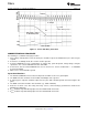
Figure 17. Turnon with Noisy Power Rail
SUMMARIZED DESIGN PROCEDURE
The following is a summarized design procedure:
1. Noise voltage and impedance at the A and C pins should be kept low. A minimum 0.01 μF or more may be
required.
2. Select C
(BYP)
as 2200 pF, X7R, 25-V or 50-V ceramic capacitor.
3. Select the MOSFET based on considerations of voltage drop, power dissipated, voltage ratings, and gate
capacitance. See sections: MOSFET Selection and RSET.
4. Select R
(RSET)
based on which MOSFET was chosen and reverse current considerations – see MOSFET
Selection and RSET.
5. Make sure to connect RSVD to ground
Layout Considerations
1. The TPS2419, MOSFET, and associated components should be used over a ground plane.
2. The GND connection should be short and wide, with multiple vias to ground.
3. A and C bypass capacitors should be adjacent to the pins with a minimal ground connection length to the
plane.
4. The GATE connection should be short and wide (e.g., 0.025" minimum).
5. Route the A and C sense lines away from noisy sources, and avoid large ground bounce between the
MOSFET and TPS2419.
6. R
(SET)
should be kept immediately adjacent to the TPS2419 with short leads.
7. C
(BYP)
should be kept immediately adjacent to the TPS2419 with short leads.
16 Copyright © 2010–2011, Texas Instruments Incorporated
Product Folder Link(s): TPS2419