
Datasheet


0.100 x 0.060
& 3 18 mil vias to
inner plane 2
10 mil trace
0.100 x 0.175
& 5 18 mil vias
0.185 x 0.045
& 3 18 mil vias
0.07 x 0.08
0.08 x 0.250
0.15 x 0.15
10 mil trace
50 mil trace
C
OUT
V
IN
: 0.00925in
2
& 3 x 0.018in vias
V
OUT
: 0.041in
2
total
0.050in trace
4 x 0.01in vias
C
IN
GND: 0.052in
2
Total
& 3 x 0.018in vias
C
IN
V
IN
: 0.0145in
2
area
& 2 x 0.018in vias
GND: 0.056in
2
total area
& 3 x 0.018in vias
C
OUT
V
OUT
: 0.048in
2
total area
5 x 0.01in vias
0.050in trace
TPS20xxC, TPS20xxC-2
www.ti.com
SLVSAU6G –JUNE 2011–REVISED JULY 2013
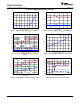
Figure 43. DBV Package PCB Layout Example Figure 44. DGN Package PCB Layout Example
Figure 45. DGK Package PCB Layout Example
The following procedure requires iteration because power loss is due to the internal MOSFET I
2
× R
DS(ON)
, and
R
DS(ON)
is a function of the junction temperature. As an initial estimate, use the R
DS(ON)
at 125°C from the
TYPICAL CHARACTERISTICS, and the preferred package thermal resistance for the preferred board
construction from the THERMAL INFORMATION table.
T
J
= T
A
+ ((I
OUT
2
x R
DS(ON)
) x θ
JA
) (1)
Where:
I
OUT
= rated OUT pin current (A)
R
DS(ON)
= Power switch on-resistance at an assumed T
J
(Ω)
T
A
= Maximum ambient temperature (°C)
T
J
= Maximum junction temperature (°C)
θ
JA
= Thermal resistance (°C/W)
If the calculated T
J
is substantially different from the original assumption, estimate a new value of R
DS(ON)
using
the typical characteristic plot and recalculate.
If the resulting T
J
is not less than 125°C, try a PCB construction and/or package with lower θ
JA
.
Copyright © 2011–2013, Texas Instruments Incorporated Submit Documentation Feedback 17