
Datasheet


www.ti.com
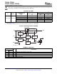
DETAILED DESCRIPTION
POWER SWITCH
CHARGE PUMP
DRIVER
ENABLE (EN)
OVERCURRENT ( OC)
CURRENT SENSE
THERMAL SENSE
UNDERVOLTAGE LOCKOUT
TPS2030 , TPS2031
TPS2032 , TPS2033 , TPS2034
SLVS190C – DECEMBER 1998 – REVISED OCTOBER 2007
The power switch is an N-channel MOSFET with a maximum on-state resistance of 50 m Ω (V
I(IN)
= 5 V).
Configured as a high-side switch, the power switch prevents current flow from OUT to IN and IN to OUT when
disabled.
An internal charge pump supplies power to the driver circuit and provides the necessary voltage to pull the gate
of the MOSFET above the source. The charge pump operates from input voltages as low as 2.7 V and requires
very little supply current.
The driver controls the gate voltage of the power switch. To limit large current surges and reduce the associated
electromagnetic interference (EMI) produced, the driver incorporates circuitry that controls the rise times and fall
times of the output voltage. The rise and fall times are typically in the 2-ms to 9-ms range.
The logic enable disables the power switch, the bias for the charge pump, driver, and other circuitry to reduce the
supply current to less than 10 μ A when a logic low is present on EN . A logic high input on EN restores bias to
the drive and control circuits and turns the power on. The enable input is compatible with both TTL and CMOS
logic levels.
The OC open drain output is asserted (active low) when an overcurrent or overtemperature condition is
encountered. The output will remain asserted until the overcurrent or overtemperature condition is removed.
A sense FET monitors the current supplied to the load. The sense FET measures current more efficiently than
conventional resistance methods. When an overload or short circuit is encountered, the current-sense circuitry
sends a control signal to the driver. The driver, in turn, reduces the gate voltage and drives the power FET into
its saturation region, which switches the output into a constant current mode and holds the current constant while
varying the voltage on the load.
An internal thermal-sense circuit shuts off the power switch when the junction temperature rises to approximately
140 ° C. Hysteresis is built into the thermal sense circuit. After the device has cooled approximately 20 ° C, the
switch turns back on. The switch continues to cycle off and on until the fault is removed.
A voltage sense circuit monitors the input voltage. When the input voltage is below approximately 2 V, a control
signal turns off the power switch.
Copyright © 1998 – 2007, Texas Instruments Incorporated Submit Documentation Feedback 3
Product Folder Link(s): TPS2030 TPS2031 TPS2032 TPS2033 TPS2034