
Datasheet


SCLK
DIN
1 2 3 4 5 6 7 8
D7 D6 D5 D4 D3 D2 D1 D0
CS
TPL0501
www.ti.com
SLIS136A –SEPTEMBER 2011– REVISED SEPTEMBER 2011
APPLICATION INFORMATION
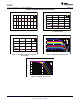
SPI Digital Interface
The TPL0501 uses a 3-wire SPI compatible serial data interface. This write-only interface has three inputs:
chip-select (CS), data clock (SCLK), and data input (DIN). Drive CS low to enable the serial interface and clock
data synchronously into the shift register on each SCLK rising edge. After loading data into the shift register,
drive CS high to latch the data into the appropriate potentiometer control register and disable the serial interface.
Keep CS low during the entire serial data stream to avoid corruption of the data.
Register Map:
Bit 7 6 5 4 3 2 1 0
MSB LSB
D7 D6 D5 D4 D3 D2 D1 D0
SPI WRITE SEQUENCE
Copyright © 2011, Texas Instruments Incorporated Submit Documentation Feedback 7
Product Folder Link(s) :TPL0501