
Datasheet


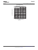


INN
INP
GAIN0
SHUTDOWN
PGND
VCLAMP
BSN
PV
CC
OUTN
OUTN
PGND
V
CC
VREF
BYPASS
COSC
ROSC
AGND
AGND
BSP
PV
CC
OUTP
GAIN1
OUTP
PGND
PowerPAD
1
2
3
4
5
6
7
8
9
10
11
12
24
23
22
21
20
19
18
17
16
15
14
13
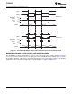
R3
51 Ω
C9
0.22 µF
C6
1 µF
D1
V
CC
C12
220 pF
C11
1 µF
C3
1 µF
C4
1 µF
V
CC
L2
(Ferrite
Bead)
L1
(Ferrite
Bead)
C15
1 nF
C14
1 nF
D2
R2
51 Ω
C8
0.22 µF
C5
1 µF
C7
10 µF
C10
1 µF
C1
0.47 µF
C2 0.47 µF
IN–
IN+
GAIN SELECT
GAIN SELECT
SHUTDOWN
CONTROL
U1
TPA3001D1
L1, L2: Fair-Rite, Part Number 2512067007Y3
D1, D2: Diodes, Inc., Part Number B130
V
CC
R1
120 kΩ
TPA3001D1
SLOS398E –DECEMBER 2002–REVISED AUGUST 2010
www.ti.com
APPLICATION INFORMATION
APPLICATION CIRCUIT
Figure 30. Typical Application Circuit
CLASS-D OPERATION
This section focuses on the class-D operation of the TPA3001D1.
TRADITIONAL CLASS-D MODULATION SCHEME
The traditional class-D modulation scheme, which is used in the TPA032D0x family, has a differential output
where each output is 180 degrees out of phase and changes from ground to the supply voltage, V
CC
. Therefore,
the differential prefiltered output varies between positive and negative V
CC
, where filtered 50% duty cycle yields 0
V across the load. The traditional class-D modulation scheme with voltage and current waveforms is shown in
Figure 31. Note that even at an average of 0 V across the load (50% duty cycle), the current to the load is high,
causing high loss, thus causing a high supply current.
14 Submit Documentation Feedback Copyright © 2002–2010, Texas Instruments Incorporated
Product Folder Link(s): TPA3001D1