
Datasheet


Functional Description (Continued)
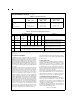
TABLE 1. Programmable Register Instructions
Function Byte 1 (Note 1) Byte 2 (Note 1)
76543210 76543210
Single Byte Power-Up/Down PXXXXX0X None
Write Control Register P 000001X See
Table 2
Read-Back Control Register P 000011X See
Table 2
Write to Interface Latch Register P 000101X See
Table 4
Read Interface Latch Register P 000111X See
Table 4
Write Latch Direction Register P 001001X See
Table 3
Read Latch Direction Register P 001011X See
Table 3
Write Receive Gain Register P 010001X See
Table 8
Read Receive Gain Register P 010011X See
Table 8
Write Transmit Gain Register P 010101X See
Table 7
Read Transmit Gain Register P 010111X See
Table 7
Write Receive Time-Slot/Port P 100101X See
Table 6
Read-Back Receive Time-Slot/Port P 100111X See
Table 6
Write Transmit Time-Slot/Port P 101001X See
Table 6
Read-Back Transmit Time-Slot/Port P 101011X See
Table 6
Write Hybrid Balance Register 1 P 011001X
Derive from
Optimization
Routine in
TP3077SW
Program
Read Hybrid Balance Register 1 P 011011X
Write Hybrid Balance Register 2 P 011101X
Read Hybrid Balance Register 2 P 011111X
Write Hybrid Balance Register 3 P 100001X
Read Hybrid Balance Register 3 P 100011X
Note 1: Bit 7 of bytes 1 and 2 is always the first bit clocked into or out from the CI, CO or CI/O pin. X
=
don’t care.
Note 2: “P” is the power-up/down control bit, see “Power-Up/Down Control” section. (“0”
=
Power Up, “1”
=
Power Down)
Note 3: Other register address codes are invalid and should not be used.
SERIAL CONTROL PORT
Control information and data are written into or read-back
from COMBO II via the serial control port consisting of the
control clock CCLK, the serial data input/output CI/O, (or
separate input, CI, and output, CO, on the TP3070 only), and
the Chip Select input, CS. All control instructions require 2
bytes, as listed in
Table 1
, with the exception of a single byte
power-up/down command. The byte 1 bits are used as fol-
lows: bit 7 specifies power up or power down; bits 6, 5, 4 and
3 specify the register address; bit 2 specifies whether the in-
struction is read or write; bit 1 specifies a one or two byte in-
struction; and bit 0 is not used.
To shift control data into COMBO II, CCLK must be pulsed 8
times while CS is low. Data on the CI/O (or CI) input is
shifted into the serial input register on the falling edge of
each CCLK pulse. After all data is shifted in, the contents of
the input shift register are decoded, and may indicate that a
2nd byte of control data will follow. This second byte may ei-
ther be defined by a second byte-wide CS pulse or may fol-
low the first contiguously, i.e. it is not mandatory for CS to re-
turn high between the first and second control bytes. At the
end of CCLK8 in the 2nd control byte the data is loaded into
the appropriate programmable register. CS may remain low
continuously when programming successive registers, if de-
sired. However, CS should be set high when no data trans-
fers are in progress.
To readback Interface Latch data or status information from
COMBO II, the first byte of the appropriate instruction is
strobed in while CS is low, as defined in
Table 1
. CS must be
kept low, or be taken low again for a further 8 CCLK cycles,
during which the data is shifted onto the CO or CI/O pin on
the rising edges of CCLK. When CS is high the CO or CI/O
pin is in the high-impedance TRI-STATE, enabling the CI/O
pins of many devices to be multiplexed together.
If CS returns high during either byte 1 or byte 2 before all
eight CCLK pulses of that byte occur, both the bit count and
byte count are reset and register contents are not affected.
This prevents loss of synchronization in the control interface
as well as corruption of register data due to processor inter-
rupt or other problem. When CS returns low again, the de-
vice will be ready to accept bit 1 of byte 1 of a new instruc-
tion.
Programmable Functions
1.0 POWER-UP/DOWN CONTROL
Following power-on initialization, power-up and power-down
control may be accomplished by writing any of the control in-
structions listed in
Table 1
into COMBO II with the “P” bit set
to “0” for power-up or “1” for power-down. Normally it is rec-
ommended that all programmable functions be initially pro-
grammed while the device is powered down. Power state
control can then be included with the last programming in-
struction or the separate single-byte instruction. Any of the
programmable registers may also be modified while the de-
www.national.com5