
Datasheet


TMS320F28335, TMS320F28334, TMS320F28332
TMS320F28235, TMS320F28234, TMS320F28232
SPRS439M –JUNE 2007–REVISED AUGUST 2012
www.ti.com
3.6.1.2 PLL-Based Clock Module
The devices have an on-chip, PLL-based clock module. This module provides all the necessary clocking
signals for the device, as well as control for low-power mode entry. The PLL has a 4-bit ratio control
PLLCR[DIV] to select different CPU clock rates. The watchdog module should be disabled before writing
to the PLLCR register. It can be re-enabled (if need be) after the PLL module has stabilized, which takes
131072 OSCCLK cycles. The input clock and PLLCR[DIV] bits should be chosen in such a way that the
output frequency of the PLL (VCOCLK) does not exceed 300 MHz.
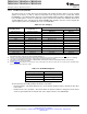
Table 3-17. PLL Settings
(1)
SYSCLKOUT (CLKIN)
PLLCR[DIV] VALUE
(2) (3)
PLLSTS[DIVSEL] = 0 or 1
PLLSTS[DIVSEL] = 2 PLLSTS[DIVSEL] = 3
(4)
0000 (PLL bypass) OSCCLK/4 (Default) OSCCLK/2 OSCCLK
0001 (OSCCLK * 1)/4 (OSCCLK * 1)/2 –
0010 (OSCCLK * 2)/4 (OSCCLK * 2)/2 –
0011 (OSCCLK * 3)/4 (OSCCLK * 3)/2 –
0100 (OSCCLK * 4)/4 (OSCCLK * 4)/2 –
0101 (OSCCLK * 5)/4 (OSCCLK * 5)/2 –
0110 (OSCCLK * 6)/4 (OSCCLK * 6)/2 –
0111 (OSCCLK * 7)/4 (OSCCLK * 7)/2 –
1000 (OSCCLK * 8)/4 (OSCCLK * 8)/2 –
1001 (OSCCLK * 9)/4 (OSCCLK * 9)/2 –
1010 (OSCCLK * 10)/4 (OSCCLK * 10)/2 –
1011 – 1111 Reserved Reserved Reserved
(1) By default, PLLSTS[DIVSEL] is configured for /4. (The boot ROM changes this to /2.) PLLSTS[DIVSEL] must be 0 before writing to the
PLLCR and should be changed only after PLLSTS[PLLLOCKS] = 1.
(2) The PLL control register (PLLCR) and PLL Status Register (PLLSTS) are reset to their default state by the XRS signal or a watchdog
reset only. A reset issued by the debugger or the missing clock detect logic have no effect.
(3) This register is EALLOW protected. See the TMS320x2833x, 2823x System Control and Interrupts Reference Guide (literature
numberSPRUFB0 ) for more information.
(4) A divider at the output of the PLL is necessary to ensure correct duty cycle of the clock fed to the core. For this reason, a DIVSEL value
of 3 is not allowed when the PLL is active.
Table 3-18. CLKIN Divide Options
PLLSTS [DIVSEL] CLKIN DIVIDE
0 /4
1 /4
2 /2
3 /1
(1)
(1) This mode can be used only when the PLL is bypassed or off.
The PLL-based clock module provides two modes of operation:
• Crystal-operation - This mode allows the use of an external crystal/resonator to provide the time base
to the device.
• External clock source operation - This mode allows the internal oscillator to be bypassed. The device
clocks are generated from an external clock source input on the X1 or the XCLKIN pin.
60 Functional Overview Copyright © 2007–2012, Texas Instruments Incorporated
Submit Documentation Feedback
Product Folder Link(s): TMS320F28335 TMS320F28334 TMS320F28332 TMS320F28235 TMS320F28234
TMS320F28232