
Datasheet


ADC Power Up Delay
ADC Ready for Conversions
PWDNBG
PWDNREF
PWDNADC
Request for
ADC
Conversion
t
d(BGR)
t
d(PWD)
TMS320F28335, TMS320F28334, TMS320F28332
TMS320F28235, TMS320F28234, TMS320F28232
SPRS439M –JUNE 2007–REVISED AUGUST 2012
www.ti.com
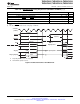
6.15.1 ADC Power-Up Control Bit Timing
Figure 6-31. ADC Power-Up Control Bit Timing
Table 6-51. ADC Power-Up Delays
PARAMETER
(1)
MIN TYP MAX UNIT
t
d(BGR)
Delay time for band gap reference to be stable. Bits 7 and 6 of the ADCTRL3 5 ms
register (ADCBGRFDN1/0) must be set to 1 before the PWDNADC bit is enabled.
t
d(PWD)
Delay time for power-down control to be stable. Bit delay time for band-gap 20 50 μs
reference to be stable. Bits 7 and 6 of the ADCTRL3 register (ADCBGRFDN1/0)
1 ms
must be set to 1 before the PWDNADC bit is enabled. Bit 5 of the ADCTRL3
register (PWDNADC) must be set to 1 before any ADC conversions are initiated.
(1) Timings maintain compatibility to the 281x ADC module. The 2833x/2823x ADC also supports driving all 3 bits at the same time and
waiting t
d(BGR)
ms before first conversion.
Table 6-52. Typical Current Consumption for Different ADC Configurations (at 25-MHz ADCCLK)
(1) (2)
ADC OPERATING MODE CONDITIONS V
DDA18
V
DDA3.3
UNIT
Mode A (Operational Mode): 30 2 mA
• BG and REF enabled
• PWD disabled
Mode B: 9 0.5 mA
• ADC clock enabled
• BG and REF enabled
• PWD enabled
Mode C: 5 20 μA
• ADC clock enabled
• BG and REF disabled
• PWD enabled
Mode D: 5 15 μA
• ADC clock disabled
• BG and REF disabled
• PWD enabled
(1) Test Conditions:
SYSCLKOUT = 150 MHz
ADC module clock = 25 MHz
ADC performing a continuous conversion of all 16 channels in Mode A
(2) V
DDA18
includes current into V
DD1A18
and V
DD2A18
. V
DDA3.3
includes current into V
DDA2
and V
DDAIO
.
170 Electrical Specifications Copyright © 2007–2012, Texas Instruments Incorporated
Submit Documentation Feedback
Product Folder Link(s): TMS320F28335 TMS320F28334 TMS320F28332 TMS320F28235 TMS320F28234
TMS320F28232