
Datasheet


GPxDAT (read)
Input
Qualification
GPxMUX1/2
High-Impedance
Output Control
GPIOx pin
XRS
0 = Input, 1 = Output
Low-Power
Modes Block
01
10
11
01
10
11
01
10
11
GPxPUD
Internal
Pullup
= Default at Reset
External Interrupt
MUX
Peripheral 3 Input
Peripheral 3 Output Enable
Peripheral 2 Output Enable
Peripheral 1 Output Enable
Peripheral 3 Output
Peripheral 2 Output
Peripheral 1 Output
Peripheral 2 Input
Peripheral 1 Input
N/C
GPxDIR (latch)
GPxDAT (latch)
Asynchronous
path
Asynchronous path
LPMCR0
GPIOLMPSEL
GPxCTRL
GPxQSEL1/2
GPIOXNMISEL
GPIOXINT7SEL
GPIOXINT3SEL
GPIOXINT2SEL
GPIOXINT1SEL
GPxSET
GPxCLEAR
GPxTOGGLE
00
00
00
PIE
TMS320F28335, TMS320F28334, TMS320F28332
TMS320F28235, TMS320F28234, TMS320F28232
SPRS439M –JUNE 2007–REVISED AUGUST 2012
www.ti.com
A. x stands for the port, either A or B. For example, GPxDIR refers to either the GPADIR and GPBDIR register
depending on the particular GPIO pin selected.
B. GPxDAT latch/read are accessed at the same memory location.
C. This is a generic GPIO MUX block diagram. Not all options may be applicable for all GPIO pins. See the
TMS320x2833x, 2823x System Control and Interrupts Reference Guide (literature number SPRUFB0 ) for pin-specific
variations.
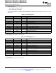
Figure 4-18. GPIO MUX Block Diagram
100 Peripherals Copyright © 2007–2012, Texas Instruments Incorporated
Submit Documentation Feedback
Product Folder Link(s): TMS320F28335 TMS320F28334 TMS320F28332 TMS320F28235 TMS320F28234
TMS320F28232