
Datasheet


X1
XCLKIN
(3.3-Vclockinput
fromexternal
oscillator)
On-chip
oscillator
X2
PLLSTS[OSCOFF]
OSCCLK
PLL
VCOCLK
4-bitMultiplierPLLCR[DIV]
OSCCLKor
VCOCLK
CLKIN
OSCCLK
0
PLLSTS[PLLOFF]
n
n ≠ 0
PLLSTS[DIVSEL]
/1
/2
/4
External
Crystalor
Resonator
To
CPU
TMS320F28335, TMS320F28334, TMS320F28332
TMS320F28235, TMS320F28234, TMS320F28232
SPRS439M –JUNE 2007–REVISED AUGUST 2012
www.ti.com
The PLL, clocking, watchdog and low-power modes, are controlled by the registers listed in Table 3-16.
Table 3-16. PLL, Clocking, Watchdog, and Low-Power Mode Registers
NAME ADDRESS SIZE (x16) DESCRIPTION
PLLSTS 0x00 7011 1 PLL Status Register
Reserved 0x00 7012 – 0x00 7018 7 Reserved
Reserved 0x00 7019 1 Reserved
HISPCP 0x00 701A 1 High-Speed Peripheral Clock Pre-Scaler Register
LOSPCP 0x00 701B 1 Low-Speed Peripheral Clock Pre-Scaler Register
PCLKCR0 0x00 701C 1 Peripheral Clock Control Register 0
PCLKCR1 0x00 701D 1 Peripheral Clock Control Register 1
LPMCR0 0x00 701E 1 Low Power Mode Control Register 0
Reserved 0x00 701F 1 Reserved
PCLKCR3 0x00 7020 1 Peripheral Clock Control Register 3
PLLCR 0x00 7021 1 PLL Control Register
SCSR 0x00 7022 1 System Control and Status Register
WDCNTR 0x00 7023 1 Watchdog Counter Register
Reserved 0x00 7024 1 Reserved
WDKEY 0x00 7025 1 Watchdog Reset Key Register
Reserved 0x00 7026 – 0x00 7028 3 Reserved
WDCR 0x00 7029 1 Watchdog Control Register
Reserved 0x00 702A – 0x00 702D 4 Reserved
MAPCNF 0x00 702E 1 ePWM/HRPWM Re-map Register
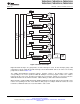
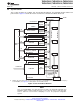
3.6.1 OSC and PLL Block
Figure 3-9 shows the OSC and PLL block.
Figure 3-9. OSC and PLL Block Diagram
The on-chip oscillator circuit enables a crystal/resonator to be attached to the 2833x/2823x devices using
the X1 and X2 pins. If the on-chip oscillator is not used, an external oscillator can be used in either one of
the following configurations:
1. A 3.3-V external oscillator can be directly connected to the XCLKIN pin. The X2 pin should be left
unconnected and the X1 pin tied low. The logic-high level in this case should not exceed V
DDIO
.
2. A 1.9-V (1.8-V for 100 MHz devices) external oscillator can be directly connected to the X1 pin. The X2
pin should be left unconnected and the XCLKIN pin tied low. The logic-high level in this case should
not exceed V
DD
.
58 Functional Overview Copyright © 2007–2012, Texas Instruments Incorporated
Submit Documentation Feedback
Product Folder Link(s): TMS320F28335 TMS320F28334 TMS320F28332 TMS320F28235 TMS320F28234
TMS320F28232