
Datasheet


Result Registers
EVB
S/W
ADC Control Registers
70B7h
70B0h
70AFh
70A8h
Result Reg 15
Result Reg 8
Result Reg 7
Result Reg 1
Result Reg 0
12-Bit
ADC
Module
Analog
MUX
EVA
S/W
ADCINA0
ADCINA7
ADCINB0
ADCINB7
ADCSOC
System
Control Block
High-Speed
Prescaler
HSPCLK
C28x
SYSCLKOUT
S/H
S/H
ADCENCLK
Sequencer 2Sequencer 1
SOCSOC
TMS320F2810, TMS320F2811, TMS320F2812
TMS320C2810, TMS320C2811, TMS320C2812
SPRS174T –APRIL 2001–REVISED MAY 2012
www.ti.com
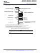
Figure 4-4. Block Diagram of the F281x and C281x ADC Module
To obtain the specified accuracy of the ADC, proper board layout is critical. To the best extent possible,
traces leading to the ADCIN pins should not run in close proximity to the digital signal paths. This is to
minimize switching noise on the digital lines from getting coupled to the ADC inputs. Furthermore, proper
isolation techniques must be used to isolate the ADC module power pins (V
DDA1
/V
DDA2
, AVDDREFBG)
from the digital supply. For better accuracy and ESD protection, unused ADC inputs should be connected
to analog ground.
Notes:
1. The ADC registers are accessed at the SYSCLKOUT rate. The internal timing of the ADC module is
controlled by the high-speed peripheral clock (HSPCLK).
2. The behavior of the ADC module based on the state of the ADCENCLK and HALT signals is as
follows:
ADCENCLK: On reset, this signal will be low. While reset is active-low (XRS) the clock to the register
will still function. This is necessary to make sure all registers and modes go into their default reset
state. The analog module will, however, be in a low-power inactive state. As soon as reset goes high,
then the clock to the registers will be disabled. When the user sets the ADCENCLK signal high, then
the clocks to the registers will be enabled and the analog module will be enabled. There will be a
certain time delay (ms range) before the ADC is stable and can be used.
HALT: This signal only affects the analog module. It does not affect the registers. If low, the ADC
module is powered. If high, the ADC module goes into low-power mode. The HALT mode will stop the
clock to the CPU, which will stop the HSPCLK. Therefore the ADC register logic will be turned off
indirectly.
64 Peripherals Copyright © 2001–2012, Texas Instruments Incorporated
Submit Documentation Feedback
Product Folder Link(s): TMS320F2810 TMS320F2811 TMS320F2812 TMS320C2810 TMS320C2811 TMS320C2812